A method to improve the thermal management of indium phosphide (InP) double-hetero bipolar transistors (DHBTs) fabricated in a transferred-substrate technology is presented. A vapour-phase deposited diamond layer acting as a heat spreader is heterogeneously integrated into the vertical layer stack. It is observed that the diamond layer reduces the thermal resistance of a 0.8 × 5 µm2 single emitter–fifinger HBT by roughly 75% down to 1.1 K/mW which is, to the authors’ knowledge, the best value reported thus far for InP HBTs of comparable size. It is also the fifirst demonstration of heterogeneous integration of diamond into an InP HBT monolithic microwave integrated circuit.
Introduction: In the past years, the interest in applications operating in the millimetre-wave (mm-wave) to sub-terahertz frequency range has steadily increased. Owing to the unique material properties of indium phosphide (InP), with simultaneously fast electron transport and high breakdown voltage, InP double-hetero bipolar transistors (DHBTs) are a good candidate for analogue mm- and sub-mm-wave circuits delivering high radio-frequency (RF) output power. An important limit for device operation lies in the HBT’s thermal resistance Rth which not only limits the RF output power of the device, but also reduces the small signal gain through self-heating of the device.
Concept: In our transferred-substrate (TS) process, the HBT’s active semiconductor layer stack is bonded to a ceramic aluminium nitride (AlN) carrier wafer, which has a thermal conductivity of about 170 W.m−1 . K−1 . In the wafer bonding process, benzocyclobutene (BCB) is used as an adhesive polymer between the active device layers and the AlN host substrate. However, BCB exhibits only a low thermal conductivity of 0.29 W.m−1 . K−1 and therefore considerably impedes the heat flflow in the integrated layer stack. To improve the heat sinking of the HBT, a 10 µm-thick nanocrystalline diamond (NCD) layer with a thermal conductivity of 600–800 W.m−1 . K−1 is added on top of the collector microstrip wiring. Exhibiting very low dielectric losses, the diamond layer can be brought into direct contact with the collector terminal without incurring additional RF losses (see Fig. 1). The NCD layer effificiently spreads the heat generated in the HBT away from the device. From the NCD layer the heat flflow is directed through large-diameter thermal vias towards the AlN host wafer, which in turn is mounted on a heatsink.
Via holes through the diamond and the BCB bonding layers exposing the collector wiring level G2 were etched in an inductively coupled plasma with flfluorine/oxygen chemistry. Silicon nitride was used as a hard mask. To avoid excessive wafer heating during the 2 hour long plasma etch, the substrate temperature was controlled by helium back side cooling with a chuck temperature set to 20°C. The end point of the etch process was monitored by double beam in situ interferometry.
The RF performance shows only a slight degradation due to the diamond layer on top of the transistor, as is evident from Fig. 3. The average current gain cutoff frequency (fT) decreased from 358 to 321 GHz after diamond integration, and the average maximum oscillation frequency (fmax) dropped from 329 to 321 GHz only after diamond layer bonding at IC = 20 mA and VCE = 1.5 V. The decrease in fT post diamond transfer can be explained by the additional capacitive loading of the previously uncovered microstrip lines connecting the devices under test. The unilateral gain is invariant under a lossless transformation; hence fmax stays at almost the same values before and after diamond wafer bonding.
The thermal resistance of the HBT was extracted by a modifified version of Bovolon’s method using the base–emitter voltage Vbe at a constant base current Ib. Fig. 4 presents the extracted values of Rth for identical 0.8 × 5 µm2 single emitter–fifinger devices without and with the diamond heat spreader. The dissipated powers in the devices, deduced from I-V curves measured on 0.8 × 5 µm2 InP DHBTs, vary between 15 and 40 mW.

Fig1
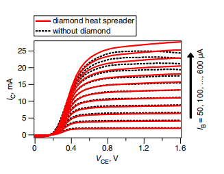
Conclusion: Improved thermal management by the inclusion of a 10 µm-thick NCD layer as a heat spreader for InP HBTs in a TS technology has been demonstrated. The NCD is heterogeneously integrated to the layer stack in a BCB adhesive wafer-level bonding process. Thermal and electrical vias through the diamond and BCB layers on top of the regular InP HBT layer stack were formed in a plasma etch process with subsequent gold via fifilling. The DC and RF behaviour of the transistors was improved mainly by enlarging the device safeoperating area. For measurement of the thermal device impedance, an extraction method based on Bovolon’s previous work was developed. With the diamond heat spreading layer, we measured a thermal resistance of 1.1 K/mW on one-fifinger HBTs of 0.8 × 5 µm2 emitter area, whereas we recorded 4.2 K/mW without the diamond. To our knowledge, this is the lowest thermal resistance for InP HBTs of similar emitter area, as compared with the previously reported record value of 1.6 K/mW.