In this paper, we demonstrate a silicon etching application of a holographically formed polymer dispersed liquid crystal (H-PDLC) photomask. H-PDLC is a periodically nanostructured material consisting of stratifified layers of polymer and liquid crystal. Due to the natural random alignment of the liquid crystal axes with respect to the polymer layers, an index of refraction mismatch exists and a reflflection occurs. Application of bias across the fifilm aligns the liquid crystals and eliminates the index mismatch causing the fifilm to become transparent. H-PDLC fifilms have been shown to suffiffifficiently attenuate the UV exposure dose in the photolithographic process when in the unbiased state, and can be electrically controlled to modulate the amount of UV transmission when electric fifield is applied. We show etch depth profifiles of patterns masked on a silicon substrate using the H-PDLC photomask device compared with etch profifiles of similar structures patterned with more conventional ink jet printed photomasks and chrome on quartz glass photomasks. We investigate reactive ion etching technique and potassium hydroxide wet etch technique.
Holographically formed polymer dispersed liquid crystal (H-PDLC) fifilms are polymeric materials formed into a microstructure consisting of stratifified layers of polymer and liquid crystal droplets. This class of fifilms possesses unique electro-optic properties including the ability to electrically modulate a band of wavelengths. Fabricated from a homogeneous mixture of photosensitive monomer and nematic liquid crystal, the material is exposed to an interference pattern where the monomer is polymerized in the bright fringes and the liquid crystal diffffuses to the dark regions. The resulting rigid structure contains periodically spaced regions of polymer and liquid crystal droplets. Due to a refractive index mismatch between the polymer layers and the randomly aligned liquid crystal rich layers a band of wavelengths related to the layer spacing is reflflected from the structure.1, 2 Reflflection wavelength described by the grating pitch is governed by the Bragg equation.
We have recently shown proof of concept of a reconfifigurable photomask device using H-PDLC fifilms as electrically controllable UV attenuators.11, 12 The photomask device in development uses H-PDLC fifilms that have been fabricated to reflflect 440 nm light, a wavelength near the peak sensitivity of Shipley 1800 series positive photoresist. By applying bias to sections of the fifilm, the user can select the regions that attenuate the exposure wavelength and regions that transmit that wavelength. Removing the electric fifield from the fifilm causes the liquid crystal droplets to return to their original state enabling the re-confifigurability of the mask. Because H-PDLC fifilms typically reflflect a 10 nm bandwidth, a 10 nm full width half maximum spectral fifilter centered at 440 nm is coupled with the fifilm to remove additional wavelengths that are emitted from a UV source. Using this system, we have previously demonstrated that a 140 mJ/cm2 dose of exposure energy can penetrate the H-PDLC fifilm in its transparent state. In its reflflecting state, the fifilm rejects approximately 60% of the exposure dose, attenuating it below the threshold for curing the 1800 series positive photoresist.
Previous work in applying liquid crystals or liquid crystal fifilms to photolithography has been done by Peng et.al and Jeon et.al. The fifirst group applied the principle of a liquid crystal display device, which relies on rotation of light polarization between crossed polarizers to attenuate the exposure dose as a photomask.13 Jeon and coworkers investigated using polymer dispersed liquid crystal fifilms (PDLC) as photomasks. PDLC does not have a reflflective state like H-PDLC, it has electrically controllable scattering and transparent states. This group used the bias-adjustable forward scattering modes of PDLC to expose difffferent rounded well profifiles. In its transparent state, PDLC exposure resulted in an etch of vertical walls.

Fig1
Photolithography was performed to fabricate features using three difffferent types of masks for comparison purposes. The fifirst mask used was a chrome patterned quartz glass mask formed using electron beam lithography. This type of lithography yields the highest resolution, but is slow and expensive to perform. The next mask was made from a pattern generated using AutoCad and printed onto an ink jet transparency. Here, the resolution is limited by the ink jet printer and is estimated to be about 50 µm. Finally, patterns were fabricated using the H-PDLC mask. Structures were fabricated using the three masking solutions on silicon and silicon dioxide wafers.
Next, a wet etch was performed. Wet etching of silicon fifirst requires patterning and etching of the SiO2 layer, then etching of the underlying silicon. The positive resist coated silicon dioxide layer was etched in buffffered HF for 12 minutes exposing the silicon below. The positive resist was removed with acetone and the silicon was etched using 45% potassium hydroxide for 8 hours. The wafers were characterized and replaced in the etching solution again for a total of 22 hours.
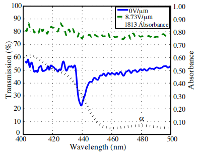
H-PDLC fifilm characterization was performed to quantify the fifilm’s optical interaction. Figure 4a displays a sample of H-PDLC transmission in unbiased and biased states. This sample shows a 35% diffffraction effiffifficiency in the unbiased state and near 80% transmission when biased with 8.73 V/µm. Figure 4b shows a characterization of transmitted intensity through the 440 nm fifilter and the H-PDLC. Superimposed curves show the amount of 440 nm light transmitted with increasing fifilm bias. These intensity curves equate to a fifilm transmission of 140 mJ/cm2 of 440 nm light while in the fully biased state, and attenuation to 35 mJ/cm2 in the reflflective or unbiased state.