One attraction of photonic crystals is the ability to control optical device characterstics by lithographically varying the geometry. In this letter, we demonstrate a 10 10 array of optically pumped two-dimensional (2-D) photonic crystal defect lasers with varying lattice parameters. By adjusting the photonic crystal interhole spacing as well as the hole diameter we are able to tune the laser wavelength from 1500 to 1625 nm on a monolithic InP–InGaAsP wafer. A wavelength resolution of 10 nm from device to device was obtainable, limited by the lithography and etching tolerances of our fabrication method.
THE use of anistropic etching techniques to form high-contrast periodic dielectric structures in which light is strongly Bragg reflected over a large angular range has been an active field of research since the first proposal made by Yablonovitch in 1987 of controllable spontaneous emission. Photonic crystals produce strong disperion of electromagnetic waves and can be engineered to diffract, guide, or trap light in spatial dimensions on the order of the wavelength of light itself. In this letter, we present recent work on lasers formed from two-dimensional (2-D) photonic crystal single defect cavities embedded in a half-wavelength thick waveguide. Simple lithographic adjustments in the cavity geometry can be used to control the wavelength, emission direction, and polarization of cavity modes. The combination of high device density, and lithographically controllable light emission make this technology interesting for a variety of laser/detector array applications such as beam-steering, beam-shaping, and multiwavelength optical signal processing.
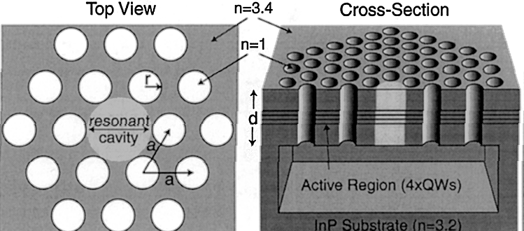
A schematic of the single defect laser cavity is shown in Fig. 1. The 2-D photonic crystal consists of a triangular array of etched air holes in a half-wavelength dielectric slab of refractive index 3.4. For an index contrast of 3.4:1 and for suitably large hole radius to lattice spacing ratio a photonic bandgap for guided modes opens up. The removal of a single hole forms a local energy well for photons, and energy is trapped in the cavity by distributed Bragg reflection off of the 2-D photonic crystal, and total internal reflection within the high refractive index slab waveguide. A number of high- cavity modes form within the frequency bandgap of the photonic crystal host. These cavity modes are highly sensitive to the local photonic crystal environment and can be wavelength tuned by adjusting the host crystal dimensions.
The epitaxy for the photonic crystal laser cavities was grown by metal-organic chemical vapor deposition (MOCVD) on InP, and contains four 0.85% compressively strained quaternary quantum wells designed for a peak emission wavelength of 1.55 m at room temperature. The final waveguide thickness is 211 nm, which is approximately a half-wavelength at 1.5 m. The photonic crystal defect cavities are formed using electron-beam lithography followed by a series of anistropic dry-etching steps, and a wet chemical etch to undercut the waveguide. An array of defect cavities was fabricated with varying lattice spacings and hole sizes in order to cover a wide range of wavelengths of the defect mode resonance. A scanning electron microsocope image of the laser array is shown in Fig. 2. The defect cavities consist of eight periods of the photonic crystal surrounding a single removed hole in the center. The patterned membrane diameter varied with the lattice spacing but was on average 8 m, and the devices were spaced by 10 m. The defect cavity lattice spacing was varied from 564 nm down to 470 nm, and for each different lattice spacing a series of devices with ratios between 0.30 and 0.40 were fabricated.

Fig1
We have demonstrated a high-density, multiwavelenth, 2-D laser array at 1.55 m based upon local defect cavities embedded in a 2-D photonic crystal host. A 125-nm laser wavelength tuning range was obtainable through lithographic control of the lattice parameters of the 2-D photonic crystal. A wavelength spacing of 10 nm between devices was achieved, limited by the tolerances in our etching process. FDTD simulations of the laser cavities is also used to accurately model the tuning of the laser mode.
上一篇: 热解光刻胶碳膜的表面研究
下一篇: 低阈值光子晶体激光器