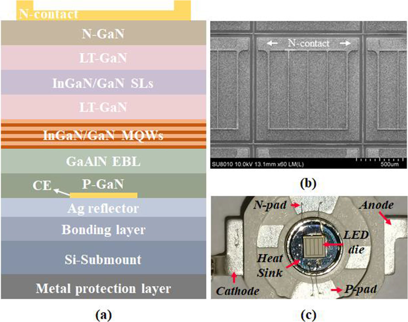
High-speed visible light communication (VLC), as a cutting-edge supplementary solution in 6G to traditional radio-frequency communication, is expected to address the tension between continuously increased demand of capacity and currently limited supply of radio-frequency spectrum resource. The main driver behind the high-speed VLC is the presence of light emitting diode (LED) which not only offers energy-efficient lighting, but also provides a cost-efficient alternative to the VLC transmitter with superior modulation potential. Particularly, the InGaN/GaN LED grown on Si substrate is a promising VLC transmitter to simultaneously realize effective communication and illumination by virtue of beyond 10-Gbps communication capacity and Watt-level output optical power. In previous parameter optimization of Si-substrate LED, the superlattice interlayer (SL), especially its period number, is reported to be the key factor to improve the lighting performance by enhancing the wall-plug efficiency, but few efforts were made to investigate the influence of SLs on VLC performance. Therefore, to optimize the VLC performance of Si-substrate LEDs, we for the first time investigated the impact of the SL period number on VLC system through experiments and theoretical derivation. The results show that more SL period number is related to higher signal-to-noise ratio (SNR) via improving the wall-plug efficiency. In addition, by using Levin-Campello bit and power loading technology, we achieved a record-breaking data rate of 3.37 Gbps over 1.2-m free-space VLC link under given optimal SL period number, which, to the best of our knowledge, is the highest data rate for a Si-substrate LED-based VLC system.
As the emergence of the innovative technologies requiring for ultra-high communication data rate (such as artificial intelligence, virtual reality and the Internet of Things), the wireless communication research focus has gradually moved to 6G, which is likely to offer a two orders of magnitude bit-rate growth over 5G . The current wireless communication network suffers from shortage of radio-frequency (RF) spectrum resources, hardly to reach giga-bit-per-second data rate. Hence, visible light communication (VLC) is rapidly emerging as a promising supplementary technology for RF communication , which can provide wide unlicensed spectrum resource (ranging from 400 to 800 THz) to alleviate the “Wi-Fi spectrum crunch” issue. Additionally, using light-emitting-diode (LED) as VLC transmitter dramatically saves the cost compared to that of laser-based system, and thus making LED-based VLC system a popular and accessible wireless communication configuration. Currently, the LED-based VLC system has reached the data rate of Mega-bit-per-second using off-the-shelf LEDs , but these LEDs are originally designed for daily lighting where their bandwidth is only several Mega-Hertz (MHz) . If the LED is well designed (e.g. reducing LED area), the achievable data rate could reach Giga-bit-per-second level . That’s to say, novel LED design or parameter optimization is critical to further increase data rate. Specifically, the InGaN/GaN vertical LED grown on silicon (Si) substrate, known as Si-substrate LED, is a promising alternative to high-speed VLC transmitter, which could not only support over 10-Gbps VLC underwater link , but also offer effective white-light illumination thanks to its Watt-level output optical power and the competitive external quantum efficiency within all visible light spectrum.
Before the Si-substrate LED is deeply investigated, due to the lack of large-size GaN bulk substrate with structural perfection, the commercial InGaN-based LEDs are normally grown on sapphire and SiC substrates. Sapphire is currently the most commonly used substrate for commercial LED fabrication, but it still imposes constraint on the GaN film quality due to its poor thermal conductivity, relatively high thermalexpansion coefficient mismatch (7.5%) and lattice mismatch (15.7%) to GaN.When high current is injected into the LED grown on sapphire substrate, sapphire prevents the efficient dissipation of heat generated by the non-radiative recombination process in LEDs. Excess heat accumulation would significantly inhibit the LED performance, causing undesired droop effect and light efficiency decrease. In addition, the LED on a sapphire substrate requires all contacts must be placed on the top side owning to the insulating property of sapphire if the GaN film is not lifted off from the sapphire substrate. Such a lateral structure complicates the contact and package schemes. The operation voltage is also increased because of the induced serious current crowding and current droop effect under this LED configuration.
To overcome these problems, plenty of innovative optimization methods were proposed to modify the structure of Si-substrate LEDs, such as the low-temperature AlN: Si interlayers technology, the step-graded AlGaN intermediate layers technology and patterned Si substrate selective-area-growth technology , etc. These technologies markedly increased the EQE of Si-substrate LEDs, especially for green and yellow LEDs. The wall-plug efficiency (WPE) of 565-nm yellow Si-substrate LEDs has reached 24.3% at the current density of 20 A/cm2 , which is the highest WPE of yellow LED to the best of knowledge.

Fig1
To evaluate the VLC performance of the Si-substrate LED with different SL period number, a VLC experiment setup is established as the illustration of Fig. 2a). A 16 GSa/s arbitrary waveform generator (AWG, Keysight M8190A) is used to generate an analog signal stream. A constant-resistance symmetrical bridged-T amplitude preequalizer (Pre-Eq.) is followed to expand the bandwidth of the transmitter. After amplified by an electronic amplifier (EA, mini circuits ZHL-6A-S+), the signal is coupled with the direct current (DC) by a bias tee (mini circuits ZFBT-4R2GW-FT+) to drive the lighting of the LED sample. Two plano-convex lenses placed in front of the LED and one plano-convex lens are used to guide the emitted light onto the PINphotodetector (PIN-PD, HAMAMATSU S10784). To prevent the saturation effect of PIN-PD, an adjustable neutral-density filter (ND filter) is placed between the PIN-PD and the lens at the receiver side. Subsequently, the converted electrical signal outputted from the PIN-PD is amplified by a trans-impedance amplifier (TIA). Its two differential outputs are connected to two EAs for the second-class amplification for a minimum of the quantization error of the oscilloscope (OSC, Agilent MSO9054A), which is followed at the end of the receiver. The utilized devices and system configuration are shown in Fig. 2b-d).