A fabrication technique by KOH etching for very thin free standing plane parallel silicon bridges in a {111} silicon wafer is presented. The applications of such a stress free slab as an evanescent optical waveguide sensor of unusually high sensitivity are discussed.
Integrated optical devices are increasingly being used in (bio-)chemical sensing applications. Usually, a change of absorption or the change of refractive index caused by an analyte above the waveguide sensor surface is monitored. The main design task for each application is to find a structure which maximizes the sensitivity on the quantity to be measured. It has recently been shown that a symmetrical waveguide with a large contrast between the waveguide index and the surrounding medium exhibits an unusually high sensitivity. In the case of a water or gas cover, a very large contrast is obtained by using a pure silicon waveguide.
Several authors have reported on various techniques for making optical waveguides in or on crystalline silicon. Planar and rib waveguides formed from silicon-oninsulator (SOI) have exhibited losses significantly lower than 1 dB/cm, in the 1.3 to 1.55 mm wavelength range. Free carrier plasma dispersion has been demonstrated in silicon waveguides as a method of modulating the refractive index. The combination of these attractive features with the ease of device fabrication using well established silicon microelectronic processing is leading to a growing interest in SOI integrated optical circuits for optical sensor and communication applications. In this work, an alternative procedure, and different processes have been developed for producing single crystal silicon waveguides. These consist of very thin free standing silicon bridges defined on a standard <111> oriented silicon wafer. We show in this letter that such bridge waveguide structure (which has mostly been considered so far for photonic band gap research) exhibits highly sensitive features which can profitably be used in shorter term sensor applications.
The material is a <111> orientation silicon wafer. Commercial standard wafers usually are cut 1o ± 0.5o off-axis. This means that the <111> crystal orientation is not perfectly parallel to the surface of the wafer. Wafers of more precise orientation can be ordered, but even these will never be cut parallel to the <111> direction at the atomic scale. In order to fabricate plan parallel silicon bridges, we start with a KOH pre-etching step to obtain a wafer surface perfectly parallel to the <111> crystal orientation as shown in figure 1 a). To that end, a masking layer of silicon nitride is deposited on the <111> oriented wafer. Then a photolithography step and a dry etching of the nitride define an opening on the silicon surface. Immersing the wafer in 25 wt% KOH at 70 ℃, the <111> plane is revealed. The etching rate is slow and depends on the angle between the <111> plane and the wafer surface. For standard wafers presenting an angle of 1o ± 0.5o the etching rate to find the <111> plane is about 2 mm/min. Once the pre-etching step is ended and the new wafer surface is a <111> plane, the silicon nitride layer is removed in 50% HF.
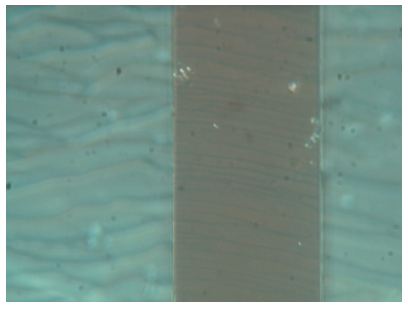
In order to assess the potential use of such bridges as optical elements a measurement of the residual roughness, resulting from the etching process, has been made. Figures 3 a) and b) show an AFM scan and a microscope picture of the top of a bridge respectively. A surface roughness of 2.4 nm, after the KOH pre-etching step, was measured. The microscope picture shows a uniform surface. In order to make a scan of the surface of the underside of a bridge, an adhesive tape was stuck on the top of a bridge. Tearing it away made the bottom side accessible. Figure 4 presents an AFM scan a) and a microscope picture b) of the bottom of a bridge. The RMS roughness is 2 nm and the surface doesn’t show any staircase resemblance. Using Marcuse’s perturbation analysis, Rickman calculated the scattering loss for a silicon core/air clad planar waveguide. For a 1 mm thickness and a 20 nm roughness waveguide, the scattering losses at 1.523 m m for the TE0 mode are about 40 dB/cm. However, interface induced scattering is proportional to the square of the roughness, so, the proposed process, characterized by a roughness of 2 nm, can be expected to lead to scattering losses significantly lower than 1 dB/cm.

Fig1
In contrast with the SOI technology, the slab silicon waveguide technology presented here uses standard wafers. It primarily leads to waveguides of high contrast. Applications in the communications field have already been proposed such as a large FSR microring resonator dropping filters at 1.55 mm wavelength. It is probably in the field of sensors, where manufacturing cost is a key factor, that the proposed technology for the fabrication of symmetrical waveguides using a standard <111> wafer is the most promising. Silicon is transparent in the wavelength range of the mid-IR where a large number of gases have strong absorption bands. Long interaction lengths are possible and the scattering effects of the residual roughness is dramatically reduced. Such characteristics are attractive for environmental applications.
A low cost process for producing symmetrical single crystal silicon slab waveguides is described. The resulting structure has the potential of becoming a building block for a number of optical microsystems such as unusually large sensitivity evanescent sensors as well as modulators, resonators and filters. The described technology is a complement to the better known SOI based waveguide technology and can also be a lower cost alternative.