This paper provides a study on the substrate effect on the opto-microwave behavior of Silicon-Germanium Heterojunction bipolar Photo-Transistors (HPT). An OptoMicrowave Scanning Near Field Optical Microscopy (OMSNOM) is performed to observe the distribution of photocurrent and dynamic behavior over the structure of the phototransistor. The photocurrent generated in the photodiode created by a n++ sub-collector and p+ substrate is extracted and analyzed. A maximum substrate diode current of 700ȝ A is observed at 850nm with a related cutoff frequency of 0.42GHz. We have extracted low frequency responsivity (at 50MHz) bandwidth product of 109.2 MHzA/W. Finally, this study will provide a design guide line for Si base phototransistors.
Nowaday’s wireless technologies have been developed to replace wire lines installed in the Home Area Network (HAN). The increase of new services and wireless devices leads us towards high data rate reaching Giga bits per second. For this purpose, new wireless network standards arise such as the IEEE802.11.ad which is the extension of the Wi-Fi toward the millimeter wave ranges (60GHz). However, the propagation is limiting to a single room, due to both the high propagation attenuation at 60GHz and to the wall absorption and reflections . Therefore, an infrastructure is needed to cover the whole home area so as to distribute the signal from one room to another one. As a result an interest has been recently put to Radio-over-Fiber (RoF) home area network application , for which low cost silicon based optoelectronics are highly desirable. SiGe hetrojunction bipolar phototransistor (SiGe HPT) are potential candidates for light detection that were proposed first in 2003 to be integrated in standard SiGe HBT technology. Since then, several laboratories are working on SiGe HPTs using different industrial process technologies like TSMC, AMS SiGe BiCMOS and IBM SiGe BiCMOS. Hybrid photoreceiver based on SiGe HPT for 60 GHz intermediatefrequency RoF applications was implemented in.
This paper investigates the effect of the substrate photodiode created by the p type substrate and n++ sub collector on the dynamic response the HPT. It also provides relavat information interms of bandwidth responsivity product to be used this HPT into microwave photonics applications. Finally a conclusion will be made on the design aspects of SiGe/Si HPT structure.
The SiGe phototransistor (HPT) was fabricated using the existing SiGe2RF Telefunken GmbH SiGe Bipolar process technology. Indeed, the phototransistor fabrication does not modify the vertical stacks of layers that are used to define a standard SiGe2RF HBT technology. This ensures the compatibility with the process technology and potential integration of complete OE-RF circuits.
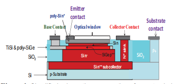
The basic HPT structure is designed by extending the emitter, base and collector layers of the reference HBT. The optical opening is made through the emitter. To improve the optical illumination, the superficial Silicon oxide and nitride layers on top of the defined optical window are removed by using Reactive-Ion Etching (RIE) process. A cross-section representation of the phototransistor structure is given in Figure 1. The light paths goes through the polysilicon of the emitter before entering the Si emitter, SiGe base and Si collector region. This HPT is essentially one large HBT whose emitter metallization was removed on the side.

Fig1
By using the bench setup described in [13], we perform the experimental mapping of the HPT at two different bias conditions (photodiode (PD) and phototransistor mode) and, also, at different optical probe position. For this study, we use a multimode optical source at 850nm and optical probe in order to make sure that our study is more realistic for HAN application where multimode source and fiber is used. The phototransistor mode is studied at a fixed collector-emitter voltage of 3V and fixed base emitter voltage of 0.857V. The photodiode mode is studied by setting collector emitter voltage of 3V and base emitter voltage of 0V. These biasing conditions are the optimum biasing conditions in terms of opto-microwave responsivity.
The base current mapping is symmetric along both x and y axis as shown in Figure 3 in both HPT (a) and PD (b) mode. In HPT mode, the sign of the base current is changed when the optical probe is moving in to the center of the phototransistor. The negative sign, when the active area is illuminated, indicates that parts of holes generated in the active area are flowing out through the base contact. However, parts of the holes are moving to the emitter for transistor amplification. In the PD mode, Ib has negative sign at all position of the optical probe as there is no any transistor action, all the holes generated are flowing out through the base contact. The base current (Ib) measured in PD mode operation is the sum of the dark current and the photogenerated current. Thus, the photocurrent generated in the structure, called the primary photocurrent, can be computed from the difference between the base current measured with and without light illumination.
The peaks of the substrate photocurrent can be explained from the vertical and lateral structure of the HPT shown in Figure 1. When the optical probe moves over the structure, the optical beam passes through different stacks depending on the position of the probe. The two peaks of the substrate photocurrent, one near the collector contact and the other near the base contact, are due to the illumination of the photodiode created by n++ sub-collector and p type Si substrate.
Figure 7 shows the frequency behavior of HPT at the center of the optical window. We recognize a slope close to -20dB / decade in phototransistor mode, characteristic of the behavior of HPT, while the photodiode mode has a slope of about -10 dB/decade. The latter characterizes the behavior of the substrate, due to the difference in transit time of the photocarriers based on the detection depth into the substrate.
上一篇: 衬底二极管对硅锗光电晶体管性能的影响
下一篇: 迈向硅芯片上锗光源的单片集成