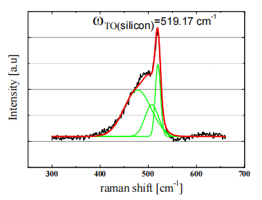
Hydrogenated doped silicon thin films deposited using RF (13.56 MHz) PECVD were studied in detail using micro Raman spectroscopy to investigate the impact of doping gas flow, film thickness, and substrate type on the film characteristics. In particular, by deconvoluting the micro Raman spectra into amorphous and crystalline components, qualitative and quantitative information such as bond angle disorder, bond length, film stress, and film crystallinity can be determined. By selecting the optimum doped silicon thin film deposition conditions, and combining our p-doped and n-doped silicon thin films in different heterojunction structures, we demonstrate both (i) an efficient field effect passivation and (ii) further improvement to c-Si/a-Si:H(i) interface defect density with observed improvement in implied open-circuit voltage VOC and minority carrier lifetimes across all injections levels of interest. In particular, the heterojunction structure (a-Si:H(p)/a-Si:H(i)/c-Si(n)/a-Si:H(i)/a-Si:H(p)) demonstrates a minority carrier lifetime of 2.4 ms at an injection level of 1015 cm−3 , and a high implied open-circuit voltage of 725 mV. Simulation studies reveal a strong dependence of the interface defect density Dit on the heterojunction silicon wafer solar cell performance, affected by the deposition conditions of the overlying doped silicon thin film layers. Using our films, and a fitted Dit of 5 × 1010 cm−2 ·eV−1 , we demonstrate that a solar cell efficiency of ~22.5% can be potentially achievable.
Heterojunction with intrinsic thin layer (HIT) solar cells has proven to be a suitable candidate for cost reduction in industrial high efficiency crystalline silicon (c-Si) wafer solar cells, due to the significantly lower thermal budget requirements, allowing the usage of much thinner wafers (<100 µm). In fact, Panasonic has recently attained record conversion efficiencies of 24.7% for a wafer size of 101.8 cm2 and 98 µm thick. To achieve higher conversion efficiency of heterojunction silicon wafer solar cells, the optimisation of the heavily doped thin-film emitter and back surface field (BSF) layers are important.
Moreover, it was found through a series of H2 effusion experiments , that the addition of doped silicon thin films may lower the passivation quality due to Fermi energy dependent Si-H bond rupture in the a-Si:H films, for either type of doping. This can result in silicon dangling bonds creation, counteracting intentional doping of the a-Si:H matrix and reduce the field effect passivation. Increasing doping concentration is also associated with increased defect densities, which results in Fermi level pinning, and linked to enhanced recombination at the a-Si:H/c-Si interface . Hence, the optimisation of the doped silicon thin film layers is essential to its application in heterojunction silicon wafer solar cells. Despite the challenges, the successful application of doped microcrystalline silicon thin film to heterojunction silicon wafer solar cells has been demonstrated. Various characterisation techniques are available for silicon thin film layers. In this paper, we highlight how the usage of μ-Raman spectroscopy has been instrumental in our optimisation process to achieve device quality doped silicon thin films, while not degrading the underlying intrinsic buffer layer and its c-Si/a-Si:H(i) interface quality.
Firstly, to investigate the impact of doping concentration on the film, the doping gas flow (B2H6 and PH3) has been varied from 1 sccm to 4 sccm, while maintaining the film thickness at ~40 nm as seen in Tables 1 and 2 below. Secondly, we investigate the impact of increasing thickness for one of the chosen deposition conditions on the μ-Raman results. Thirdly, given that the heterojunction silicon wafer solar cell typically consists of a symmetrical thin intrinsic a-Si:H layer for passivation before the deposition of the thin doped layers, we also investigate the impact of substrate type on doped silicon thin film growth (i.e.: intrinsic a-Si:H and glass substrates). The doped silicon thin film on an a-Si:H substrate is prepared by depositing a thin intrinsic a-Si:H layer of ~5 nm on a microscopic glass substrate before depositing the doped layers of ~10 nm with different hydrogen dilution ratios R = H2/SiH4. In all depositions, the RF power density, deposition pressure p, and substrate temperature T were maintained at 0.07 W/cm2 , 1.9 Torr, and 180˚C respectively.

Fig1
Our extracted film crystallinity and conductivity as a function of doping flow provides an alternative support to the above claims, and highlights the importance of doping flow optimisation amid other deposition parameters. The optimum doping gas flow for the p-doped silicon thin film and n-doped silicon thin film was found to be B2H6 = 2.2 sccm and PH3 = 2 sccm respectively. At such doping flow, a sufficiently high conductivity for the p-doped and n-doped thin film is achievable at 1.8 S/cm and 16 S/cm respectively. Increasing doping flow beyond the optimum point will only increase non-electrically active dopant atoms, which can act as recombination centers for minority carriers in a solar cell device, hence reducing the current collection efficiency.
Secondly, with the chosen deposition conditions as per sample P6 with a B2H6 doping gas flow of 2.0 sccm, several p-doped silicon thin film samples were deposited on microscopic glass substrates with varying thickness from 20 nm up till 100 nm in 20 nm steps. Figure 7 shows the µ-Raman spectra of these samples, while Figure 8 shows the corresponding plot of film crystallinity and conductivity. It is clear from Figures 7 and 8 that as the film thickness increase from 20 nm to 100 nm, the film evolves from a purely amorphous phase into a microcrystalline phase in which film crystallinity χc increases from 1% to 42%. This change correlates well with an increase in conductivity from 0.06 to 4.8 S/cm.
上一篇: 表面声波器件在碳化硅上使用铌酸锂
下一篇: 用于高性能柔性电子产品的超薄芯片