Separately and about the same time, Noyce came up with a similar design whichbecame known as the monolithic integrated circuit. His approach was more practical forfabrication by using a planar semiconducting substrate with oxidation and diffusionprocesses to create the circuits and used evaporated metal to form the connections betweencircuits. The planar process revolutionized the way electronics were made and thecomplexity of functions that could be combined into a single circuit. Thereby, circuitvolume, power dissipation, and wiring parasitic effects were dramatically reduced. Afterthe revolution in circuit miniaturization, the demand for cost-effective memory devices andintegrated circuits for computers generate the semiconductor industry in the 1970s [6]. Theglobal semiconductor integrated circuits sales reached $360.27 Billion in 2020 and theindustry is expected to grow more[7]. Since their origins, the speed, and capacity ofintegrated circuits have progressed enormously; driven by the ability to pattern smallfeatures in order to fit more and more transistors on chips of the same size [6].
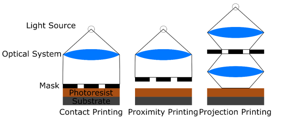
After the development of the integrated circuit, the fabrication process evolveddrastically. Improvement in resolution of fabrication process has been the main drivingforce, because a better resolution allows miniaturization of electronic components, whichresults in more chips per wafer, smaller circuit size, and higher performance devices.Furthermore, a better resolution improves productivity and thus reduces cost. Thus, the fabrication process requires the ability to pattern complex structures at high resolutionyield and throughput [8]. Photolithography has been the dominant patterning process,which has until recently kept up with the stringent technology requirements of integratedcircuit manufacturing process [9].

Fig1
For example, as chip became more complex, there was advancement in mask makingprocess. As resolution requirements continuously grew, reduction lithography, whichprints a reduced image on the wafer, was developed. Reduction lithography eliminatedmaking 1:1 1 masks, but required an additional step which aligns the reduced image ontothe wafer thus improvements in metrology were inevitably required. Furthermore, asresolution and image area grew, this new process put a burden on lens manufacture byrequiring dramatic increases in lens size and complexity. Lastly, changing the illuminationsource was necessary for a better resolution, which required a change of optical materials,photoresist materials, chemistry and processes, as well as the improvement developmenttools [9].
Extreme ultraviolet (EUV) lithography is one of next generation lithography, whichfollowed the above development process with several unexperienced challenges [8]. EUVlithography enhanced resolution by using soft X-ray wavelength. First, EUV lithographytools must operate in high vacuum and only incorporate reflective optical elements(including photomasks), because EUV wavelengths cannot penetrate through significantlyany medium. Since every EUV reflective surface absorbs ~ 30%, creation of a highpowered EUV light source is necessary. Since photons coming from high power EUVsources can severely heat the tool, thermal stability of pellicles and heat extraction fromvacuum raise engineering challenges. As can be seen, improvement in photolithographyis challenge because each component in lithography tool is interconnected [8].
While several nanopatterning techniques have been proposed by researchers, EUVlithography and ultraviolet nanoimprint lithography (UVNIL) are the only ones which havecommercial potential for semiconductor production [8]. Nanoimprint lithography (NIL) isan emerging technique which is an effective and low-cost nanoscale patterning method anda promising solution to the practical limits of photolithography [6, 8]. A general NILprocess is illustrated in Figure. 1.3. Before imprinting, the imprint resist is dispensed onthe substrate. The template mask is lowered onto the monomer droplets of resist, and thedroplets spread and fill the relief patterns in the mask by capillary action. The resist dropsmerge and completely fill the features on the template. A photo-curable or thermallycurable polymer resist reproduces the pattern after curing. The template mask is removed,leaving an imprinted resist on the substrate. Ideally, imprinted resist conforms completelywith original template. This pattern can then be used for further processing such as reactiveion etch. The NIL process offers a low cost method for mass producing nanoscale featuresand has the potential to become a key nanolithography method for future manufacturing ofintegrated circuits.
上一篇: 晶圆级单晶金刚石的常用工艺
下一篇: 晶圆干燥的基础和技术