Impressive advances in the epitaxial growth of III-nitridecompound semiconductors have recently been made. Thesesemiconductors have been widely used in both electronicdevices and optoelectronic devices. III-nitride compoundsemiconductors possess excellent properties that includewide band gap, high critical breakdown field, and high electron saturation velocity, which have encouraged the rapiddevelopment of III-nitride-based transistors over the pastdecade.1–3 However, the power-handling capability of thesedevices still suffers from the leakage current through theSchottky gate. Furthermore, the long-term thermal stabilityof Schottky contacts to III-nitride semiconductors has not yetbeen achieved at high temperatures. To reduce the gate leakage current, increase the high breakdown voltage, and operate more reliably at a high temperature, metal–oxide–semiconductor ~MOS! or metal–insulator–semiconductorstructures are being widely investigated. In previous reports,a number of gate dielectrics such as AlN,4 SiO2 ,5 Si3N4 ,6Ta2O5 ,7 and Ga2O3 (Gd2O3)8 have been used in the MOSstructures. However, the grown external dielectric layerswere contaminated by surface contaminants from the originalsemiconductor. Furthermore, the associated stoichometricstructure was greatly influenced by the growth conditions.Foreign contaminants of the Ga oxide/GaN structure can beavoided, if Ga oxide can be grown on GaN layer directly. Inthis research, a photoelectrochemical method utilizing aHe–Cd laser was used to grow Ga oxide on n-type GaN andthe performance of the resultant MOS varactor devices wasdemonstrated.
The epitaxial layers used in MOS devices were grownon c-plane ~0001! sapphire substrates using a metalorganicchemical vapor deposition system. Trimethylgallium and ammonia were used as the Ga and the N sources, respectively. Silane was used as the Si source for the n-type dopant. Anundoped GaN buffer layer, with a thickness of 800 nm, wasgrown on a sapphire substrate at 520 °C, followed by thegrowth of a 600 nm thick Si-doped GaN layer at 1050 °C.Using Hall measurements performed at room temperature,the electron concentration and mobility were found to be3.2231017 cm23 and 350 cm2/V s, respectively.
The schematic configuration of the MOS varactor deviceis shown in Fig. 1. To remove native oxide from the n-typeGaN surface, the samples were etched by aquaregia for 10min. Ohmic Ti/Al/Pt/Au ~25/100/50/200 nm! metals wereevaporated using an electron-beam evaporator. After the liftoff process, concentric ohmic contact rings ~inner radius5150 mm, outer radius5400 mm) were patterned and thenthermally annealed by rapid thermal annealing in a N2 ambient at 700 °C for 1 min. To grow the Ga oxide layer onn-type GaN, the samples were oxidized in a chemical solution of H3PO4 with a pH value of 3.5 by illuminating themwith a He–Cd laser. The Ga oxide was identified as Ga2O3by energy dispersive spectrometer measurements. The thickness of the grown Ga2O3 layer was 100 nm, according to thea-step measurement. A 200 nm thick Al circular pattern with a radius of 100 mm was defined using photoresist andaligned on the center of the Ga2O3 layer.
Figure 2 shows the current–voltage characteristics of theMOS devices measured by an HP4145B semiconductor parameter analyzer. It can be seen that the forward and reversebreakdown voltages are 28 V ~corresponding breakdownfield52.80 MV/cm) and 57 V ~corresponding breakdownfield55.70 MV/cm), respectively. The breakdown voltage isdefined as the voltage where a rapid increase of corresponding leakage current occurs. When a forward bias is applied,many electrons in the n-type GaN accumulate at the interfacebetween the Ga2O3 layer and the n-type GaN. However,when a reverse bias is applied to the MOS device, few holecarriers will accumulate at the Ga2O3 /n-type GaN interface.Therefore, the reverse breakdown voltage is larger than theforward breakdown voltage. This carrier accumulation phenomena can also explain the fact that the reverse leakagecurrent is smaller than the forward leakage current, as seen inFig. 2.

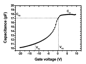
In summary, we report on the growth of a Ga2O3 layerdirectly on n-type GaN using a photoelectrochemical methodby the application of a He–Cd laser. MOS devices were fabricated with the oxidized n-type GaN samples. The forwardand reverse breakdown electric fields of the grown Ga2O3layer were 2.80 MV/cm and 5.70 MV/cm, respectively. Thedensity of the interface states of the Ga2O3 /n-type GaN was2.5331011 cm22 eV21. An extremely low reverse leakagecurrent of 200 pA operated at 220 V was achieved. We thus see that Ga2O3 layers grown by this photoelectrochemicaloxidation method using He–Cd laser illumination are suitable for inversion layer formation. This MOS structure appears to be a promising candidate for applications of GaNmetal–oxide–semiconductor field-effect transistors.