ABSTRACT
GaN and related semiconductors have become an increasingly prominent material for a wide range of active and passive devices from optoelectronics to high frequency and power electronics as well as photocatalysis. Regardless of the application, anisotropic etching is required for micro and nano structuring, currently performed by reactive ion etching (RIE). Alternately, metal-assisted chemical etching (MacEtch) is an open-circuit plasma-free anisotropic etching method that has demonstrated high aspect ratio device structures devoid of plasma-induced damage found in RIE. This paper presents an in-depth study of the ensemble electrochemical mechanisms that govern the photo-enhanced MacEtch process of GaN and related heterojunctions. Through in-depth experimental investigations, modeling and simulations, the effects of local cathode and anode design, energy-band alignments, and solution chemistry on MacEtch are correlated with the underlying electronic mechanisms of carrier generation, annihilation, transport, and extraction, establishing a fundamental framework for parametrized prediction of system behavior. These findings carry profound implications for tailored design of photoelectrochemical processes employed not just for uniformly etching wide/ultrawide bandgap materials but more broadly for semiconductor-based photocatalytic reactions in general. One-pot photo-enhanced MacEtching of AlInGaN multi-heterojunction device structures including superlattices and multiquantum wells are demonstrated.
I. INTRODUCTION
GaN and other III-nitride semiconductors continue to push the boundaries for device performance in high power and frequency,as well as optoelectronic applications thanks to their wide bandgap, high electron mobility, proven heterojunctions, thermal stability, as well as strong resistance to radiation and chemical damage. The fabrication of these devices, especially with aggressively scaled dimensions, demand complex processes of which etching is a critical step. It is known that plasma-based dry etch, such as reactive ion etching causes crystal damage. In some cases, the etching-induced damage is irreversible, while in other cases, it is too deep to be removed without substantial loss of materials and sidewall profiles.Alternative etch methods are highly desirable.
Metal-assisted chemical etching (MacEtch) is an open circuit plasma-free anisotropic etching method.It relies on a local catalysis-driven charge-transfer process to enable site-controlled etching with the distinct advantage of being free of ion-induced damage. Using MacEtch, superior etching properties and unparalleled damagefree device results have been demonstrated for a wide variety of semiconductors, such as Si, Ge, III-As, III-P,III-N,SiC,and Ga2O3 and related homo- and heterojunctions. For wide and ultra-wide bandgap semiconductors, because of the limited carrier mobilities, it is necessary to use above bandgap photons (hv ) to generate free electron–hole (e- –h+) pairs and enhance MacEtch rate. The redox reaction in hv-MacEtch extracts the electrons from the semiconductor, drive charge imbalance with holes left at the surface to oxidize the semiconductor to generate porosity or etch away.
II. RESULTS AND DISCUSSION
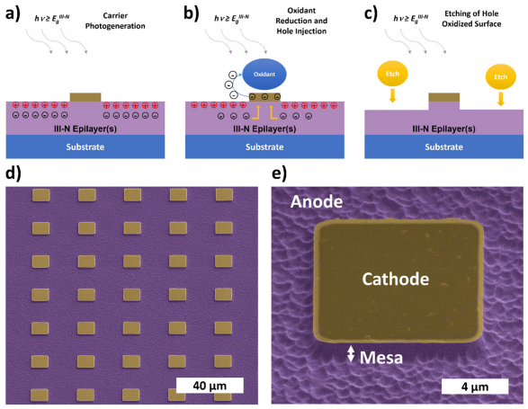
Figure 1 illustrates the hv -MacEtch process of III-Nitrides, where the metal catalyst acts as a cathode for reduction reactions and the semiconductor plays the role of the anode for oxidation reactions. hv -MacEtch proceeds via photogeneration of free carriers in illuminated material as illustrated in Fig. 1(a). A metal catalyst (cathode) that is patterned on the semiconductor surface acts as a reduction mediator, transferring free electrons to an oxidant species present in the solution; in this case a persulfate (S2O8 2-) ion, which drives electron–hole pair separation as shown in Fig. 1(b) and is critical in preventing recombination. Continuous reduction of the oxidant species effectively acts as a charge sink with a potential bias allowing electron current to flow from the semiconductor to the cathode and then to the solution until the aqueous oxidant supply is exhausted. In addition to this, the metal patterns also block incoming light preventing photogeneration from occurring in the region immediately beneath the patterns. The local circuit is “completed” by the injection of remaining hole species to the nitride surface which oxidizes the material via bond reorganization.The etchant within the solution proceeds to remove the III-N oxide as shown in Fig. 1(c). The combined act of surface oxidation and etching acts as the counter-process to the reduction-driven electron sink but for holes instead. The process repeats until it is terminated. Etch termination can occur via several pathways that are either chemical, electrical, or electrochemical in nature: quenching of the reaction, loss of illumination as well as etch stops that are chemically inert or electrically inactive. For simple reference of half reactions involving carriers, the reader is referred to Bardwell et al. that provides a likely set of electrochemical equations with KOH as the etchant. It is noted that the exact stoichiometry is still unknown and is the subject of ongoing study.

Fig1
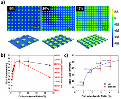
To study the effect of geometry, we first vary the spacing between catalyst features. Figure 2(a) shows three structures produced by MacEtch. In these structures, the square array of catalyst patterns maintains a constant feature size of 10 lm, while the spacing varies from 18, 10, and 5 lm, resulting in corresponding C:A ratios of 10%, 20%, and 45% from left to right, respectively.
As the C:A ratio is increased from 1% to 45% as shown in Fig. 2(b), we find that the etch rate is maximized at around 10% and slowly tapers off as the C:A ratio approaches 45%. When the etch rate is converted to a volumetric scale (right Y axis), i.e., the total amount of material removed, the observed trend as a function of C:A ratio both in rising and falling edges are amplified. While the etch rate reduced only by less than 10% (from 55 to 50 nm/min) from C:A ratios of 10% to 45%, the volumetric removal rate dropped by 50% (from 21 000 to 14 000 lm3 /s). The volumetric scale is more representative of the overall electrochemical reaction as compared to traditionally reported etch rates, as can be seen from Fig. 2(a) where the increased feature packing density (from left to right) clearly shows that the actual volume removed is smaller. Under the etch condition specified, the inflection point for material removal rate is at just below a C: A ratio of 10%. The etch rate behavior observed is a result of the competition between the rate of hole injection, which increases with cathode area and the photogeneration of electrons and holes, which is proportional to the anode area. The C:A ratio is thus a reflection of photoelectrochemical (PEC) conversion with the peak position reflecting the maximum PEC system efficiency. As such, the C:A ratio is a coupled function of chemical reaction efficiency (oxidation, reduction, corrosion and mass transport) as well as photoelectronic conversion efficiency (carrier generation, transport and extraction).

Fig2
Additionally, we also study the effect of the C:A ratio at different feature dimensions. Figure 2(c) plots the etch rate as a function of C:A ratio in the range of 1%–4%, with both micrometer and submicrometer catalyst features (precise feature sizes labeled next to the data points). Over this range, the etch rate is enhanced with increasing C:A ratio, consistent with an electron extraction rate limited regime where an increase in cathode size allows for higher electron extraction and hole injection, leading to higher etch rate as observed previously in Fig. 2(b). Remarkably, the etch rate increase is similar for the same C:A ratio irrespective of the catalyst size, e.g., both 4 lm and 400 nm feature sizes yield about the same etch rate. The isolated effect of feature sizes with constant C:A ratio will be discussed later (Sec. II A 3).
Electronic effects on etching extend beyond the geometric design of the cathode to the material composition of the electrodes themselves. When metals are deposited on the semiconductor surface, a Schottky barrier is formed with the barrier height dictated by the work function of the metal. Electronically, it is expected that the degree of band bending from energy level alignment will dictate the degree of electron flow toward the metal electrode barring any tunneling effects. To study the influence of work function, we must first distinguish between catalytic metals (i.e., Au and Pt group metals) and noncatalytic metals.
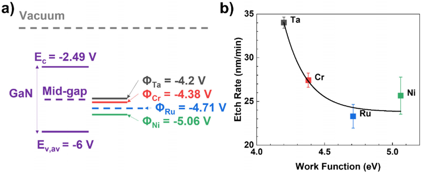
Here, the metal patterns are intentionally engineered such that they comprise of a catalytic metal capping layer (Ru) and a charge transfer layer (CTL) based on a lower work function metal such as Ta, Cr, and Ni (non-catalytic in this system). The associated energy alignments of the metal work function as well as GaN conduction and valence band edges are shown in Fig. 4(a). It is clear that all metals studied have energy alignments close to or below the mid-gap level of GaN and will cause varying degrees of upward band-bending. As the work function of the CTL (metal interlayer in direct contact with GaN) reduces from just over 5 eV to around 4.2 eV, the etch rate tends to rise (by approximately 40% in the studied range) as shown by Fig. 4(b) with an exponential dependence. From a diode operation perspective, the applied bias as well as potential barrier caused by the Schottky contact both possess an exponential dependence with current, which potentially contributes to the trend in experimental etch rate. From an electronic standpoint this corresponds to the hole injection at the semiconductor surface vs electron extraction which is what occurs at the CTL. It should be noted that the transfer of electrons from the catalyst surface to the solution is a separate affair and presents another condition that is dependent on both the chemical reactivity as well as catalytic strength of the metal.

Fig4
III. CONCLUSIONS
With the ever-increasing prevalence of nitride materials from optoelectronic to RF and power applications comes process challenges as devices continue to scale for performance enhancements. Material damage induced by conventional RIE etching proves to be a major hurdle that is often increasingly detrimental to performance as devices scale. MacEtch has proven its viability in producing structures devoid of plasma damage with a similar throughput to RIE. In this study, we demonstrate that multi-HJs can effectively be etched homogeneously via a new, one-pot HCl chemistry across the widespread AlInGaN material system ranging from superlattice structures to device structures with Al and In fractions of up to approximately 16% in each case. More fundamentally, we reveal the governing mechanics to the electrochemical process that occurs during hv -MacEtch. We identify consequential effects on carrier extraction with cathode materials and geometric design, balance between the metal cathode and semiconductor anode areas as well as energy level alignments between dissimilar material interfaces with varying metal work function and semiconductor doping-dependent fermi-levels. By correlating the above design parameters with their electronic counterparts, we establish a basic framework that allows for translation beyond the AlInGaN system to not just emerging nitride materials such as AlScN but other wide bandgap semiconductors such as SiC and ß-Ga2O3, all of which have been shown or are expected to follow the hv-MacEtch process. Crucially, the electronic effects studied in this work enables system-specific modeling of carrier extraction. This can be on a device-by-device basis depending on both the multi-HJ structure and the geometric layout. It can also be for an application-specific basis such as photocatalysis depending on both electrode design and energy level alignments of redox processes. In summary, this study has moved the hv-MacEtch process beyond reported bulk materials to multi-HJ stacks involving materials across the AlInGaN system, demonstrating viability required for device-relevant processing of 3D nitride structures. While several manufacturing specific aspects such as reproducibility and process control require continued development, it is important to note that we have, for the first time, successfully cross-correlated process design parameters with baseline electronic effects. This significant advancement paves way for device and application specific modeling, providing a powerful prediction pathway for processing that extends beyond hv -MacEtch of nitride and wide bandgap materials to encompass other PEC systems utilizing similar electronic materials.
上一篇: 碳化硅独立光子器件的晶圆级集成
下一篇: 集成电路中金属氧化物半导体的可靠性研究