INTRODUCTION
The recent fiber telecommunication system progress and 5G wireless communications are creating demand for ultra-high speed digital devices, such as HBTs or HEMTs for ICs. These devices are fabricated on semi-insulating Fe-doped InP substrates. As performance of these devices is improved and the chip size is increased, the market expects higher quality and larger diameter substrates (6-inch) to improve device performance and reduce production costs. With the growth of larger diameter InP crystals, the increase of dislocation densities becomes critical. Though a boat growth method is the most appropriate for achieving low dislocation density, the boat growth of InP is difficult because of twinning issues. Therefore a <111>-growth orientation have been previously adopted to prevent twinning [1]. However, this type of orientation is not suitable for the production of (100) substrates.
Table1 shows a comparison of InP crystals by VCZ(Vapor pressure controlled Czochralski), VGF(Vertical Gradient Freezing) and VB(Vertical Boat) methods, respectively.
We focused on the improvement of lot size and succeeded in developing a long VB grown InP single crystal ingot. Long crystal ingot means more wafers can be obtained from one ingot. Doping concentration of impurities changes from the seed side to the tail side because of segregation phenomenon. Therefore the longer ingot makes smaller variation in doping concentration among wafers from one ingot.
We are reducing the furnace cost gradually through the simplification of the structure. In addition, productivity per furnace is gradually increasing through larger lot sizes and yield improvement.
SEI has succeeded in developing 6-inch Fe-doped InP substrates that are higher in quality and that can be manufactured at competitive costs using VB technique.
CRYSTAL GROWTH AND WAFER PROCESSING
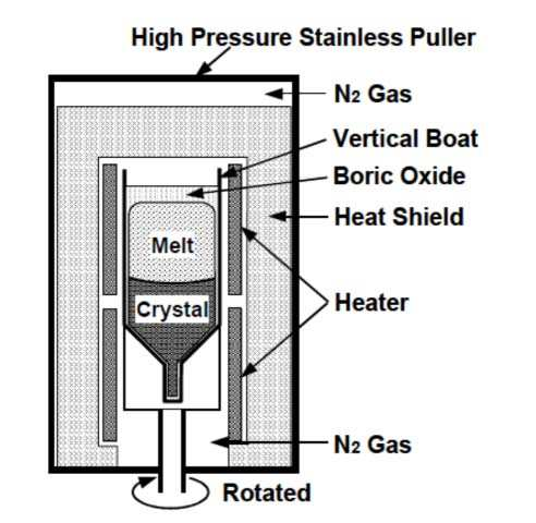
The equipment for VB single crystal growth techniques is schematically drawn in Figure 1. A single crystal is grown in a vertical boat by solidifying the melt from a seed crystal with <100>- growth orientation placed at the bottom of the vertical boat. InP single crystal can be grown under small axial temperature gradient of between 5-20 degree C /cm near the solid-liquid interface.

Figure 1.VB equipment for InP single crystal growth techniques
This makes it possible to grow InP crystals with much lower dislocation density and more reproducibility than VCZ method. The wafer processing was performed under a double side polish (DSP) and single side polish (SSP) that is almost of the same concept as 6-inch GaAs wafer processing.
