For the gate last integration scheme, dummy poly silicon gateremoval is one of the indispensable processes either for a high-kfirst or a high-k last route. In this paper, experimental results ofdummy poly silicon gate removal using TetraMethyl AmmoniumHydroxide(TMAH) chemical etching are presented. Thepreliminary results show that the poly silicon removal rate washighly sensitive to the wet etch conditions. By optimizing the wetetch conditions, high selectivity of poly silicon with respect toSiO2, SiN4 and hafnium silicon oxynitride (HfSiON) was obtainedA gate trench of critical dimension (CD) of about 70 nm withoutpoly silicon residue was fabricated using optimized conditionsThe excellent etch capability of the optimized wet etch process wasalso demonstrated by controlling trench profiles.
I. Introduction
As CMOS logic devices are scaled in their dimensions from 45 to the 32 nm node, a lotof advanced process technologies may have to be introduced to overcome barriersintroduced by pitch scaling, such as the extension of immersion lithography, mobilityenhancement technology, ultra-shallow junction technology, etc (1). In these technologies.the metal/high-k (MHK) gate stack is of great importance in many aspects such assignificantly decreasing the gate tunneling current and gate resistance, eliminating thedepletion effect of the poly silicon, the boron penetration problem for PMOSFET; andalleviating Fermi-level pinning effects (2). Two integration schemes for MHkengineering can be used. The gate first scheme, which is similar to the conventionalCMOS process, and the other is gate last scheme. By now, the gate last scheme haveprevailed over gate first schemes because the thermal stability of both the high-k andmetal gate stack can be maintained by avoiding the high temperature source/drainactivation anneal of the MHK stack (3). For the gate last scheme, we try two differentintegration routes, high-k first and metal gate last route (high-k first) and pure gate lastroute (high-k last). For the high-k first/metal gate last route, high-k is deposited beforeremoving the poly silicon dummy gate, and the deposition of the gate metal is done afterthe removal. For the high-k last route, the high-k was deposited after removing the polysilicon dummy gate, covering the bottom and the sidewalls of the gate trench. For thegate last integration scheme, the dummy poly silicon gate removal is an indispensableprocess. Both complete poly silicon removal and perfect trench profile control are keysfor the dummy poly silicon gate removal process, which will in turn affect the subsequentdeposition of the high-k for high-k last scheme or metal gate material for high-k firstscheme. This paper presents a series of experimental results of dummy poly silicon gateremoval by using TetraMethyl Ammonium Hydroxide (TMAH) chemical etching inorder to find an appropriate process to remove dummy poly silicon gate in the gate lastintegration scheme.
Il. Experimental Procedure
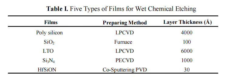
The samples were prepared on 4-inch P-type (100) oriented silicon wafers with aresistivity of 8-12 -cm. Hafnium silicon oxynitride (HfSiON) was selected as the high-kmaterial, which was prepared by co-sputtering Hf(99.999%) and Si (99.999%) targets fordeposition on silicon substrate with a thin SiO, layer (~lnm) on top in Ar/N ambiencefollowed by a rapid thermal anneal at 900 °C for 30 sec (4). Other dielectric layers weredeposited using conventional chemical vapor deposition (CVD) and furnaces. Blanketwafers of the respective films were prepared to monitor the wet chemical etch propertieswhich are summarized in Table l. Poly silicon gates of critical dimension (CD) of about70 nm were fabricated by the joint effort of a JEOL6300 E-beam tool and a LAMRainbow 4520 tool. The isolation spacers were composed of Si;N, and a low temperaturesilicon oxide (LTO). LTO was also used as the inter layer dielectric (ILD) in this paperThe electronic grade TMAH aqueous solution was used as the wet chemical for the polysilicon dummy gate. This is usually used as silicon substrate wet etch in the fabrication ofmicro-electromechanical systems (5). TMAH concentrations were varied from 10 to 25vol%, and the processing temperatures were from 50 to 80 °C. All wet etch tests wereprocessed in a quartz tank.
The thickness of the HfSiON layer was measured by a GES5E ellipsometer, and thethickness of the other dielectric layer by a NanoSPEC elcometer. The poly silicon gateremoval and trench profile after TMAH wet etching were evaluated by carrying outcross-sectional scanning electron microscopy (SEM) characterization on a Hitachi 4800.

Ill. Results and Discussion
The etch rate (ER) of poly silicon on blanket wafers in 10 vol% TMAH at differentprocess temperature is shown in Fig .1 (a). The ERs of poly silicon on blanket wafers inTMAH solution with different concentrations etched at 80 °C is summarized in Fig. 1 (b)One can see that the processing temperature had a remarkable impact on the ER, whilethe TMAH concentration had little effect on the ER. The ER increased by about 3 timeswhen the temperature changed from 50 to 80 °C in 10 vol% TMAH The ER remainedunaltered as the TMAH concentration increased from 10 to 25 vol% at 80 °C processtemperature.
上一篇: 硅片上亚微米颗粒的去除方法
下一篇: 锑化镓物理与技术