Abstract
With the trends toward larger wafer size and thelinewidth going below 100 nm, one of the challenges is to controlthe resist thickness and uniformity to a tight tolerance in order tominimize the thinfilm interference effect on the critical dimen-sion. In this paper, we propose a new approach to improve resistthickness control and uniformity through the softbake process.Using an array of thickness sensors, a multizone bakeplate, andadvanced control strategy, the temperature distribution of thebakeplate is manipulated in real time to reduce resist thicknessnonuniformity The bake temperature is also constrained to pre-vent the decomposition of a photoactive compound in the resist.We have experimentally obtained a repeatable improvement inresist thickness uniformity from wafer-to-wafer and across indi-vidual wafers. Thickness nonuniformity of less than 10 A has beenobtained. On average, there is 10 X improvement in the thicknessuniformity as compared to conventional softbake process.
I.INTRODUCTION
With shrinking feature sizes, the challenge tomaintain adequate and affordable process latitudebecomes increasingly difficult. Advances in process controland metrology will be necessary to achieve less than 10 nm(3o) gate critical dimension (CD) control, especially for 130nm and below technology node [l]. In addition to a smallerprocess window, the industry is also moving toward 300-mmwafers for economic reasons. This places a stringent demandon all the lithographic processes as the control requirement isnow stretched over a larger area. In addition, lithography onnonconventional substrates such as quartz photomask or LCDflat panel display manufacturing is also critical.Due to thin-film interference effects, CD varies with the re-sist thickness. The resist thickness has to be well controlled toremain at the the extrema of the swing curve where the sensitivity of CD to resist thickness variations is minimized. As theamplitude and periodicity of the swing curve increases with decreasing wavelength (2], the control of the resist thickness andits uniformity across alarger substrate becomes increasingly important. Already for the 200-mm substrate, resist thickness uniformity specification is met by having tight controls over important parameters such as relative humidity, temperature, spin speed, exhaust, etc. during spin coating [3]. With a larger substrate, the specifications for these parameters are expected to be even more demanding. The range of useful thicknesses for any fixed viscosity resist is also limited as the transition from laminar to turbulent flow now occurs at a lower spin speed. This transition to turbulent flow during spin coating is largely responsible for the increase in thickness nonuniformity at the edge of the wafer [4], [5]. However, it is sometimes necessary to spin the resist at a higher speed to obtain the optimum resist thickness, as indicted by the extrema of the swing curve. Taking the above considerations into account increases the complexity of the coating process.
Typical lithographic process begins with hexamethyldisilazane (HMDS ) priming, followed by resist coating and then thesoftbake process. Softbake is an important process performedafter coating the resist to remove excess solvent from the resistfilm, reduce standing waves, and relax the resist polymer chaininto an ordered matrix. As in all bake processes, temperaturecontrol [6], [7] during softbake is important. Conventionallythe resist is baked at a fixed temperature with temperaturecontrol of +1°C for consistent lithographic performance [6].However, our experiment shows that maintaining a uniformtemperature profile across the bakeplate does not reduce theresist film nonuniformity. In this paper, we propose a techniqueto control the resist thickness and improve its uniformitythrough the softbake process.
There has been some research on in situ monitoring of the resist thickness and properties during the bake process [8]–[12].To study the bake mechanism, Paniez et al. [8] used in-situ ellipsomtery while Fadda et al. [9] used contact angle measurements to monitor the resist thickness during the bake process. Morton et al. [10], [11] used in-situ ultrasonic sensors to monitor the change in resist properties to determine whether the resist has been sufficiently cured, thereby determining the endpoint of the softbake process. In related work, Metz et al. [12] used in-situ multiwavelength reflection interferometers to measure the resist thickness versus bake time to determine the optimum bake time.
For our research, we not only use the in-situ thickness mea-surements to detect the endpoint of the softbake process butalso improve the resist thickness uniformity by manipulating thebakeplate temperature distribution. Various sites on the waferare made to follow a predefined thickness trajectory to reducethickness nonuniformity to less than I nm at endpoint. The baketemperature is also constrained during softbake to prevent decomposition ofthe photoactive compound [6], [11]. On average.we have obtained about 10 x improvement in thickness unifor-mity at endpoint. Besides silicon wafers, our method may alsobe applied to photomask and flat panel display manufacturing.
II.EXPERIMENTAL SETUP
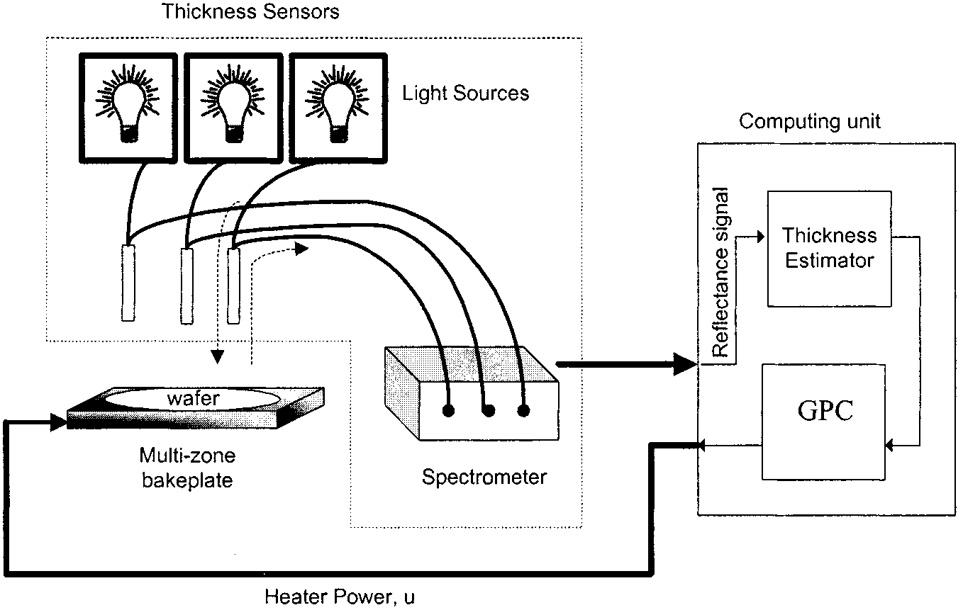
The experimental setup used to control resist thickness con-sists of three main parts (see Fig. 1): a multizone bakeplate.thickness sensors, and a computing unit. In all our experiments.commercial -line resist Shipley 3612 is spin-coated at 2000 rpmon a 4-in wafer. Thicknesses at three sites, each 1 in apart, aremonitored and controlled to demonstrate the control strategy(see Fig. 2). Fig. 3 shows the photograph of the experimentalsetup with a 4-in wafer sitting on top of the mutlizone bakeplate.

Figure 1
An array of three thickness sensors is mounted directlyabove the wafer at sites where the resist film thicknesses arebeing controlled. Currently, the setup is for a 4-in wafer (radius.2 in; 3 points monitored). This can be easily scaled to a 12-inwafer (radius: 6 in; 7 points monitored) The number of sensorsand hence the amount of computation required for 12-in waferis roughly doubled and this should not be an issue.
上一篇: 磷化铟晶片退火处理研究
下一篇: 硅上多晶磷化铟的生长和表征