ABSTRACT: New approaches for future photovoltaic cell concepts issue a challenge to crystalline wafer handlingEspecially concepts based on ultra-thin silicon wafers force automation developers to look even beyond the aims ofthe international PV manufacturing roadmap. As widely known, crystalline photovoltaic wafers are a very sensitiveobject for industrial production, especially for gripper-based handling solutions. The known wafering method'SLliM-cut requires an additional cleaning step after a single wafer was detached from the parent substrate. To cleanorganic residues off substrates an etching bath is applied. In general, the investigation takes a look on the potentiahreads for thin foils such as cleaning a particle contamination off the substrate's surface. The paper further discussesthe opportunities and limits for the automated handling of ultra-thin objects in cleaning baths and presents anapproach for a high-volume process control. The tested gripping principles and processing parameters for underwatergripping of ultra-thin wafers and the opportunities for withdrawing the ultra-thin wafers out of a liquid are presented.
INTRODUCTION
Beyond the timeline of the ITRPV in terms of waferthicknesses l] somerecent developments of newphotovoltaic concepts use ultra-thin silicon wafers (2].Thus, besides challenges for the automated handling ofthin silicon wafers for high volume production, thehandling of ultra-thin silicon substrates was researchedand developed [3].
Automated approaches for new wafer processingtechniques play a key role for an extensive exploitation ofultra-thin wafer developments. Investigations which leadfurther than pioneer developments and research successeson lab level often not include the transfer and proof ofconcept for mass manufacturing. Thus, the importancefor lowering hurdles for new concepts is the main task forautomation developers. Appropriate handling methodsand further approaches in advanced control and efficientmanufacturing in key processes will enable a quickerproduction of new or modified PV technologies.
The EU-funded project SUGAR (Silicon Substratesfrom an IntegratedAutomated Process) developed aprocess for wafering silicon ingots into ultra-thin foilsThe researchers focus not only on the integrity andcapability of the wafer and cell processing, but also onthe feasibility and applicability of automated handlingand transport. The newly developed wafering techniquerequires a wafer handling in a wet bench environmentwhere ultra-thin wafers are processed with differentliquids such as solutions or rinsing baths. Thus, theanalysis and evaluation of challenges for ultra-thin waferhandling in liquid aims at the exploitation of thecollaboratively achieved research results and will assiston bringing these project results into an industrialfiamework.
2 MATERIALS AND METHODS
The ultra-thin wafers for which the automatedhandling is developed are produced in the laboratories ofthe imec by using the “Stress induced Lift-off Method’(SLiM-Cut). This method has been developed by the PVresearchers at the imec [4] and makes particularlyefficient use of bulk material by reducing kerf loss whileproducing wafers with a thickness of around 50 um [4]Different dimensions of the wafers can be generated andthe herein handled ultra thin wafers are conditioned tosizes of 30x50 mm (recent results make use of 50x50 mmsubstrates).
While todays standard 156x156 mm wafers areprocessed in batch or inline wet bench processes theultra-thin wafers generated from the Slim-cut processmay not be transferred in the same way. Slot-wise in-cassette transportation of ultra-thin wafers will highlyrisk wafer damage due to edge loads during immersionand emersion in the process. Ultra-thin wafers becomemore flexible but also less rigid. State of the art inlinetransportation in wet benches is executed on small plasticrollers. This in-process transportation is perhaps suitablefor thin wafer conveying. A challenging issue is the smallgap between the rollers for the (currently) miniaturewafer transportation. But even large area ultra-thinsubstrates could suffer from punctual loads on the waferssurface and cracking could occur. Irregular punctual loadwill result from the tangential touch of the wafersbackside while a solution or rinsing liquid is applied onthe upside. Lateral guidance of the ultra-thin wafersduring roller transportation is a potential source ofdamage as well. Based on the handling experiments withultra-thin wafers in the course of the project, a singlewafer handling method was considered to complementthe standard wet bench processes for ultra-thin wafers. Agripping method for single substrate handling in aprocess basin was developed which is named “grippingin-liquid."
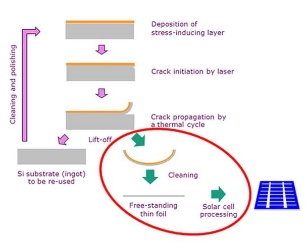
2.1 Process draft for wafer handling in liquid mediaThe collaborative elaboration of the results for a largescale production needs the development of appropriateautomated handling solutions. Figure 1 depicts the singlesteps of the process flow and the process-linkinghandling steps. The circle highlights the sequence for thegripping-in-liquid (GIL) application.

Figure 1
The considered process sequence comprises the pick-up of a coated and bowed foil which was detached froman ingot by the stress induced lift-off method. Thesubsequent cleaning of the stress inducinglayer and thefurther processing in liquid environmentcomplete thewafering process by using this SLiM-cut approach. Afterthe cleaning step the clean wafers are transported to aninspection point, which acts as the interface to the dryprocessing environment.