Abstract: Single-crystal quartz material is widely applied in the manufacture of resonators anosensors, but it is difficult to process because of its high hardness. A novel way to fabricate single-crystaquartz structures is proposed in this paper; the method includes quartz-on-silicon (OoS) technologyand inductively coupled plasma (ICP) etching, which makes it feasible to fabricate complex structureswith crystal quartz. The QoS method encompasses the bonding of silicon and quartz, followed bythe thinning and polishing of quartz, which can enable the fabrication of an ultra-thin quartz wafeion silicon. In this way instead of the conventional wet etching with hydrofluoric acid, the quartzlayer can be easily etched using the ICP dry-etching method. Then, the structure of the pure quartzmaterial is obtained by removing the silicon wafer. In addition, the silicon layer can be processed intothe appropriate structure. This aspect overcomes the difficulty of processing a complex structure olsingle-crystal quartz with different crystal orientations. Thin single-crystal quartz wafers of Z-cut witha thickness of less than 40 um were obtained by using this method, and a complex three-dimensionalstructure with an 80 um width was also acquired by the ICP etching of the quartz wafer. The methodcan be applied to make both crystal-oriented quartz-based sensors and actuators, such as quartzresonant accelerometers.
1. Introduction
Single-crystal quartz material has captured significant attention, which is attributed to itsoutstanding material properties in sensor manufacturing (1,2]. Quartz crystal not only possesses thepiezoelectric property, but also has excellent mechanical, electrical, and temperature characteristicsIt is designed and manufactured for resonators, oscillators, and filters because of its exceptionaperformance in frequency stabilization and frequency selection (3,4). Furthermore, the piezoelectricitof quartz material can be used to excite the resonators into vibration to simplify both sensor structuresand excitation circuits (5].
The strong covalent bond characteristic of single-crystal quartz material makes it difficult to alterand its high hardness and difficult processing characteristics also impede the improvement of deviceperformance. The tradiional methods used to process quartz structures mainly include fluoride-basedwet etching (6l, laser micro-/nano-processing (LMP) (7,8], and inductively coupled plasma (ICP) dryetching (9,10]. The depth of wet-etched quartz can reach 500 um (11], but because of the anisotropy ofquartz, the sidewall crystal edges can only be reduced through continuous experiments, and cannot beeliminated (12-14). Because wet etching requires a specific orientation of quartz crystal, z-cut quartz is often used for wet etching. According to the relationship between the cutling angle of the quartz crystaand the frequency-temperature characteristics, it is difficult to find the zero-temperature coefficientpoint of z-cut quartz within its working temperature range. n this case, the large temperaturehysteresis of the sensors causes an additional complicated compensation. There are always somechallenges when etching delicate and complex structures with different thicknesses using wet etchingMoreover, wet etching is not an environmentally friendly method. LMP-etched quartz ranges in depthfrom a few microns to hundreds of microns (15,16). The local high temperature of LMP may cause thequartz to lose its piezoelectric activity, which is quite detrimental, yet the width of the high-temperatureareas (over 15 um) is difficult to narrow, Furthermore, the quality factor, single frequency, and aging rateof quartz resonators are largely determined by the smoothness, parallelism, and geometric correctnessof the quartz's surface.
Inductively coupled plasma dry etching has proved effective for processing single-crystaquartz. The plasma-chemical etching process can etch a single-crystal quartz plate (z-cut) witha thickness of 369 um through windows with large linear dimensions (3 mm x 10 mm) (17)A few institutions have used ICP systems to achieve a depth of quartz of over 100 um (18,19However, small-sized structures are difficult to process in this way and have poor sidewall morphologiesAdditionally, the typical single-quartz etching depth (with better morphology) is generally less than50 um (20-22). Currently, the thickness of the single-crystal quartz wafer is generally more than 100 umFurthermore, considering the increasing fragmentation rate, the processing cost of a thinner quartzwafer will increase. Therefore, it is currently difficult to directly obtain sensors and actuators of crystalquartz using dry etching. The research on the combination of the bonding, thinning, and dry etchingof single-crystal quartz in this study aimed to solve these problems by taking advantage of dry etchingwhile avoiding its disadvantages to obtain a favorable device morphology.
2. Experimental
2.1. The Design of the Overall Process
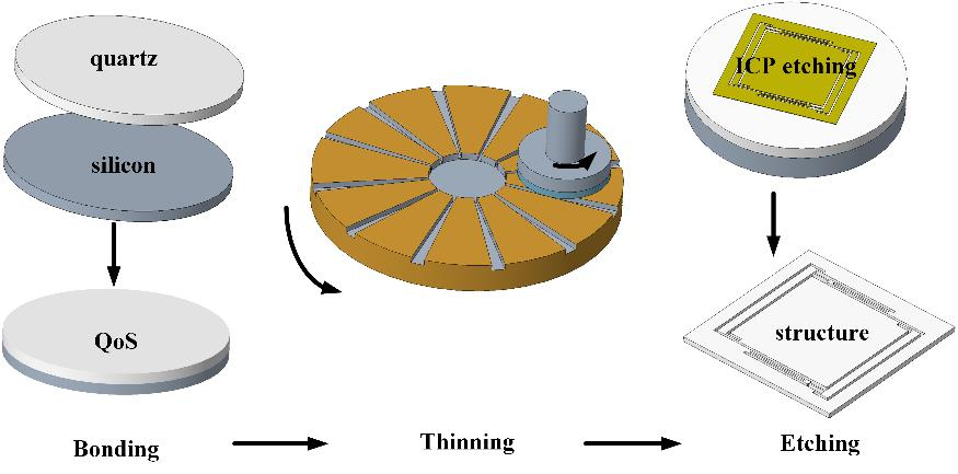
In seeking to fabricate a complex three-dimensional structure of single-crystal quartz with a goodsurface morphology, a novel processing method was proposed that covers the bonding of quartz onsilicon (OoS), the thinning and polishing of OoS, and the ICP dry etching of quartz, as shown in Figure 1.Not only was the optimized single-step procedure shown to achieve good results via a sequence ofexperiments, but the three-step process also proved capable of achieveing excellent compatibility.

Figure 1
2.2. Bonding of Quartz and Silicon
The silicon wafer was bonded with the quartz wafer via direct bonding or auxiliary bondingto obtain the OoS wafer. The original wafers selected for bonding should have a good thickness uniformity and a low surface roughness. Before bonding, the silicon and quartz wafers should becleaned ultrasonically using acetone and alcohol.
上一篇: CMP后清洁
下一篇: 氮化硅对硅和二氧化硅的高选择性蚀刻