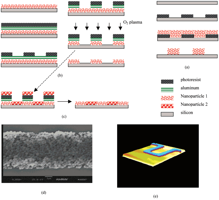
A lithographic approach to generate clean palterms of multiple types of nanoparticles on one 4-inch silicon wafer is demonstrated in thispaper. Each type of nanoparticle s precisely directed to the desired location. The process is mainly based on conventional microelectroniechniques with extremely high reproduciblity. This enables the possibility of industrial applications to fabricate devices made of nanocryslalsA thin flm of polystyrene spheres,150 nm in diameler, was first coated on the silicon wafer with laver-by-aver self- assembly. followed by aayer of aluminum deposited on the thin film. A layer of positive photoresist was spun on the surface of aluminum and then pattermed bithographic technique. The unprotected aluminum was removed by wet etching until the polystyrene thin film undermeath was exposed to theair. Oxygen plasma was employed to etch the polystyrene thin film all the way to the silicon surlace Subsequently, a thin film of another typeof nanoparticle. silica parlicle 78 nm in diameter, was adsorbed onto the surface with layer-by-ayer self-assembly. Eventualy, aluminum anophotoresist were removed and each type of nanoparticle was located next to each other as the pattern was desianed. A scanning electronmicroscope was used to produce the image of the pattern.
Introduction. Nanoparticles have been the focus of manymaterial researchers due to their unique properties in themicroelectronics, optoelectronics, and chemical fields.!,2 Agreat deal of attention has been attracted to the variouspotential applications of nanoparticles to complex nano-electronic devices, photonic crystals, and biochemicalsensors.3-7 Among numerous nanoparticle deposition tech-niques, layer-by-layer (LbL) self-assembly, since its intro-duction by Decher et al.8, has become, due to its simplicityand versatility, an increasingly popular technique, whichenables adsorption of colloidal nanoparticles onto almost anymaterial. The alternate immersion of substrate in oppositelycharged solutions allows thin films of nanoparticles, en-zymes, or protein in nanometer scale to be coated byelectrostatic interaction.
However, before the LbL self assembled nanoscale col-loidal structure is applied to real devices, an approach mustbe developed to easily generate complex and distinct patternson the multilayer films. Recently, some results have beenreported for the creation of spatially resolved nanoparticlefilms. These works are mostly based on the microprintingtechnique in which a template is first fabricated by stampingtwo functional chemicals on the flat substrate, then directingnanoparticles onto adhesion-promoting regions while they are repelled by adhesion-resisting regions.14-21 This methodis quite successful but is restrictive in application by thenecessity of special microstamps and the deliberate selectivedeposition. They are all chemical methods in principleAnother challenge prior to device fabrication is to patterntwo or more types of nanoparticles on one wafer. Hammondand T. Vossmeyer groups demonstrated their approaches tointroduce two types of nanoparticles in the matrix byselective deposition technique.
In our early reports,23,24 two methods based on thecombination of traditional lithography and LbL assemblywere presented to pattern one type ofnanoparticle film. Oneis referred to by authors as the “modified lift-ofp’, the otheras the “metal-mask method. The strategy completely differsfrom the microprinting technique, thus avoiding the difficultselective deposition. The patterns created by this strategyare illustrated in Figure 1. Since the standard 4-inch waferprocess was adopted to pattern the LbL assembled nano-particle films, dramatically high reproducibility is obtainedon the whole wafer surface. In addition, each step of Lblself-assembly can be automatically controlled: therefore. thisidea may find wide industrial application in the future. Theschemes of both methods are illustrated in Figure 1.

Figure 1
In this paper, an approach to generate patterns composedof two types of nanoparticles is presented. The approach isthe combination of metal-mask and lift-off. It provides a capability to fabricate varieties of microdevices or systemsthat consist of more than one type of nanocrystals. UV lightlithography, etching, and lift-off, which are all matureprocesses in the semiconductor industry, are used in themethod. They ensure the remarkable reliability of the methodThe flexibility of traditional lithographic technique may leadto other methods that may be developed to fulfill the sametarget. In this work, a 4-inch silicon wafer served as thesubstrate. The thin film of polystyrene nanoparticles, 150nm in diameter, were coated on the wafer with LbL self-assembly and patterned by the metal-mask method, but thealuminum and photoresist layers above the pattern were notremoved immediately. Subsequently, a layer of silica nano-particles, 78 nm in diameter, was deposited above all theselayers. Eventually, the photoresist and aluminum weredissolved in series and the silica particles that attached onphotoresist were also removed during this lift-off processThe scheme is illustrated in Figure 1(b) and (c).
Experimental Method. Polyelectrolytes were obtainedfrom Aldrich-Sigma and were used as follows: (1) poly(dimethyldiallylammonium chloride) (PDDA) aqueous solution.MW 200 to 300 K, 3 mg/mL, 0.5 M NaCl, (2) sodiumpoly(styrenesulfonate) (PSS) aqueous solution, MW 70 K3 mg/mL, 0.5 M NaCl. The blue-dyed carboxylate modifiedpolystyrene particles, 150 nm in diameter, were obtainedfrom Seradyn Inc. The polystyrene aqueous solution wasmade in dispersion to water volume ratio of 1:9. The silica nanoparticles dispersion (8 mg/ml) was diluted from Snow-Tex colloidal silica (40.9 wt %, PH 9.6, 78 nm in diameter)which was made by Nissan Chemical Industries, Ltd. Thephotoresist is Shipley AZ18 13. Electronic-Vision dual sidemask aligner EV420 from Electronic Visions, Inc. was usedas the UV light illuminator. Aluminum layers were depositedby a DV-502A high-vacuum evaporator from DentonVacuum, Inc. Dry etching was carried out using an 800 seriesmicro RIE system from Technics Inc. Ultrasonication wasperformed using an 8892 Cole-Parmer ultrasonic cleaner.
上一篇: 氮化硅对硅和二氧化硅的高选择性蚀刻
下一篇: 基于半导体异质结的光热制冷分析