ABSTRACT
Amorphous silicon carbide thin films (SiC) were produced byPECVD technique at room temperature. Post-annealing was usedto crystallize the SiC films. These films were etched in reactive ionetching system using SF + O2 gas mixtures. The influence of O2concentration in process was investigated by mass spectrometrytechnique. Using this technique, it was possible to estimate thebetter conditions where the etching rates are optimal and also toverify the contributions of etchant species like F and O on theproduction of the main volatile products SiF4, CO and CO2.
INTRODUCTION
Amorphous and crystalline SiC thin films are promising materials for highAmorphous andtemperature and high power applications, being considered a natural complement for Sias the structural material in micro and nano-electromechanical systems (MEMS) (1)because of their superior mechanical stability at high temperatures and its extraordinarchemical inertness. However, the difficulties in growing crystalline material and theimited knowledge in the areas of oxidation, doping, etching and metallization has limitedits use to very specific applications, such as light emitting devices and; specific hightemperature, high-power and high-frequency applications that are not suitable for Si orGaAs based devices (2). MEMS applications have stimulated research on depositioncharacterization and further processing of SiC (3). For microelectronic applications, SiCfilms are usually produced at low temperatures (T < 500°C) by plasma depositiontechniques, such as magnetron sputtering and plasma enhanced chemical vapordeposition (PECVD) (4). The films deposited by these techniques are generallyamorphous and can be transformed into polycrystalline by annealing at high temperaturesin inert atmospheres.
For microelectronic applications, one of the most critical technological steps is theSiC etching process. As SiC is not attacked by the most aqueous chemicals due to Si-(bonds, which are very strong, dry methods are more appropriate, being the plasma-basedetching the dry method more commonly used. Amongst the several plasma etchingtechniques, the reactive ion etching (RIE) is the most important technique used infabrication of SiC-based devices (5-7), being a complex process that involves both.chemical and physical processes (8). Fluorinated gases have been routinely emploved forSiC etching but the etching rates are too slow to be used in industrial applications. Amanner to increase these rates is the addition of O gas in the process. Using this mixture,the dissociation of fluorinated gases leads to free F atoms that react with Si atoms andform volatile SiF4, while the O, promotes the production of CO, (n = 1 or 2) leading tocarbon etch. Although. SiC etching based on fluorinated gas and oxygen have beerextensively studied the detailed etching mechanisms involved is still not fully understoodyet.
In recent years there has been an increased effort aimed to characterize etchingprocesses to improve understanding of the etch mechanisms, process control andoptimization of the plasma parameters, such as input power, gas flow rate and pressureand composition of gas mixture. For this, Langmuir probe, mass spectrometry and opticalemission spectroscopy, are frequently used, In the case of the mass spectrometry, the gasspecies produced in the etching processes can be detected, producing different spectra fordifferent conditions of the processes. The evolution of these spectra can be related to thecharacteristics of the films and it is possible to estimate the better conditions where theetching rates are optimal and also to verify the contributions of the etchant species.
In this work, thermal annealed SiC films were etched by an rf plasma in a reactive ionetching (RIE) reactor. The gases used in the process were SF and O, at different ratiosThe influence of this ratio on the etching rate of the film was studied and related to themass spectra of the discharge.
EXPERIMENTAL
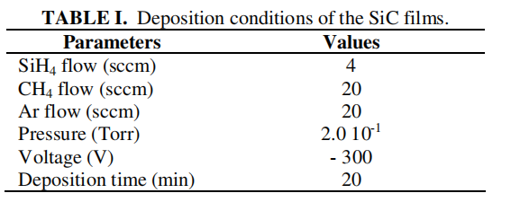
SiC thin films have been grown in an rf (13.56MHz) PECVD reactor using a CH4 +SiH, + Ar gas mixture on p-type, (100) and 1-10 2.cm silicon wafers. The substrateswere placed on a water cooled stainless steel cathode (6.5 cm in diameter) of acydindrical chamber. Samples were produced under the conditions showed in Table IAfter deposition, the thickness of each sample was measured using profilometry(TENCOR Alpha-Step 500 profilometer), resulting in an average thickness of 400 nmXRD measurements were also done in the deposited films, using diffractometer PhillipsPW 1380/80. The Si and C contents of the films were obtained from Rutherford backscattering (RBS) measurements in as-deposited films. The RBS spectra were carried outusing a 2MeV He+ beam equipment and analyzed with RUMP code (RBS spectroscopyanalysis package) developed by IR. Dolitle (9). After those characterizations, sampleswere cleaned (RCA recipe) and submitted to annealing in a conventional furnace at1000°C in N, atmosphere for 30min, The crystallization level, induced in the films, wasevaluated by XRD analysis.

The annealed samples were etched in a reactive ion etching (RIE) reactor using SF6 as the reactive fluorinated gas and O2 as an additive. The SF6/O2 ratios used were varied from 0 to 100%. All processes were taken at 25 mTorr total pressure (Pt), 12 sccm total flow, and rf power of 50 W. Substrates were maintained at 20ºC during etching. Etching experiments had been carried out on masked SiC samples during 3 min for etch rate measurements. The etching rates of the films were determined by profilometer measurements.
上一篇: GaN 表面的清洁
下一篇: 硅在HF溶液中的阳极溶解