ABSTRACT
In this paper, we have studied the microstructure evolution of one-year room-temperature-aged Through-Silicon Via (TSV) copper after annealing the TSV samples at 300 °C, 400 °C and 500 °C for 180 minutes. Hardness and elastic modulus values are obtained by using nano-indentation technique. The hardness and elastic modulus values decrease as annealing temperature increases. The microstructure of copper (Cu) is examined to obtain grain size and texture, using electron backscatter diffraction (EBSD). Copper grain growth, if any, is studied under different annealing temperatures. There was no observable grain growth for the annealing temperatures studied in this work. Moreover, microstructure variation at different locations within a Cu TSV is also studied.
INTRODUCTION
Copper through-silicon via (TSV) is an enabling technology for 3D integration, playing an important role in connecting stacked dice. Increasingly, TSVs with a diameter ranging from 100 µm, 50 µm, 10 µm, or less are being pursued by industry. The microstructure of electroplated copper will be dependent on the TSV diameter, as the diameter shrinks in size. Annealing the TSVs at high temperatures typically changes the grain size and orientation, resulting in additional changes in material properties such as hardness. Annealing the Cu TSV reduces the residual stress as well as Cu pumping and associated reliability issues in subsequent thermal excursions.
The performance of transistors is sensitive to stresses induced by the integration of Cu TSV in a chip. In metaloxide-semiconductor field-effect transistor (MOSFET) devices, a stress of 100 MPa can change the carrier mobility by over 7% [28]. There are a few studies done on the microstructure and mechanical behavior of Cu TSV after annealing [1, 26, 27], while there are a lot of studies available on the mechanical behavior and reliability aspects of Cu TSVs [2-5, 12-24]. There is only limited study on the long-term aging of Cu TSVs. In this paper, the effect of long-term aging followed by high-temperature annealing on the microstructure and mechanical properties of aged Cu TSV is experimentally studied.
SAMPLE PREPARATION
Cu TSV samples were fabricated using a conventional cleanroom process. The silicon wafer was 500 µm thick and had uniformly distributed 50-µm diameter blind TSVs with 250 µm depth. Copper was electroplated from a seed layer deposited on the side wall of a blind TSV. Upon electroplating, the silicon substrates were diced into a number of samples for molding and microstructure analysis. The over-plated Cu was not polished off. The Cu TSV samples were stored in room temperature (e.g. 25 ºC) and cross-sectioned to be characterized after one year. The cross-sectioned TSV samples were polished using colloidal silica solution and mechanical planarization to obtain a smooth planar surface. The electron backscatter diffraction (EBSD) was performed to characterize grain size and texture, while nano-indentation was performed to characterize the hardness and elastic modulus.
EXPERIMENTAL PROCEDURE
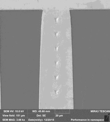
Since Cu recrystallizatio Annealing effects were studied by EBSD and Nanon occurs at 250 °C [6, 7], annealing temperature was chosen above 250 °C. This ensures that the temperature is high enough to let microstructure recrystallization. Three annealing temperatures were 300 °C, 400 °C and 500 °C with 180 minutes of annealing for each temperature. Nano-indentations were carried out using a Nano-indenter (MTS XP System® equipped with the continuous stiffness measurement attachment). During the indentation process, the applied load and the displacement were continuously recorded. A three-sided pyramidal diamond Berkovich tip to a maximum depth of 1000 nm. There are six indentations, starting from 5 µm from the top edge with a spacing of 20 µm along the axis of the TSVs (Figure 1). The spacing was selected so as to minimize the influence from other neighboring indents as well as the influence of surrounding silicon walls. The elastic modulus and hardness values were obtained from the test by using the Oliver-Pharr relation [8].

Fig 1
EBSD measurements were carried out using a TESCAN SEM® equipped with an EBSD detector. The samples were angled 70° towards the electron-scanning microscopy (SEM) detector while taking the EBSD measurements. All EBSD images were rectangular in shape with 120 um length along the axis of the TSV and 60 um width along the transverse width or radial direction of the TSV. EBSD measurements were first taken on the cross-sectioned samples, and then the samples were subjected to high-temperature annealing treatments. It is important to study the cross-sectioned samples under vacuum condition or flowing argon gas to prevent copper oxidization. Therefore, the annealing treatments were accomplished using Cambridge Fiji Plasma® atomic layer deposition (ALD) tool that is capable of providing such operating conditions. The cross-sectioned Cu TSVs were placed in the chamber with a ramp of 13 °C/minute under vacuum and flowing argon gas at 20 sccm throughout the annealing process. After letting the Cu TSVs cool down under vacuum environment, the second postannealing EBSD measurement was conducted on the same TSV. By comparing the two EBSD images, before and after annealing, the crystal structure changes due to annealing could be determined.
下一篇: APCVD法生长的硅纳米线的化学表面钝化