1. Introduction
At present time, problem of detection of low-level short duration signals at the wavelengths from 0,9 to 1,6 μm is extremely actual. The existing photodetectors do not meet the requirements of sensitivity, processing speed and resolution. One of the most preferred solution of this problem is to create vacuum photoelectronic device with photocathode based on the InP/InGaAs heterostructures [1- 2]. The purposes of the work was to obtain effective InP/InGaAs photocathode with quantum efficiency on the level of 3-5% and to implement the results of photocathode structure researches in real photodetector which works in near infrared range (NIR).
2. Сonstruction of vacuum photoelectronic device
Photosensitive device is implemented on the basis of the hybrid technology. The photocathode structure and solid-state element, as the receiver of the photoelectrons, are contained in one vacuum value. Applying of this technology simultaneously allows to register low-level signals at the wavelengths from 0,9 to 1,6 μm, to get processing speed of a device on the level of a few nanoseconds and ensure a low level of internal noise as compared to devices with non-vacuum parts. The proposed sensor construction consists of three main parts: device framework with inputs for supplying voltage and outputs, glass with fixed photocathode structure, plate with the receiver of the photoelectrons. Proximity-focusing technology was used to provide a high resolution.
The body and the all internal elements of the detector produced from the vacuum outgassing materials. Non-evaporable getters made from the titanium plates were also included in the device structure. These getters could improve the vacuum level in the working device, which is extremely important for the detector lifetime. The processes of assembling sensor and activation of photocathode structure need ultra-high vacuum conditions. All steps of sensor creation were conducted in the ultrahigh vacuum installation, which could reach the level of·10-9 Pa [3].
3. Photocathode structure
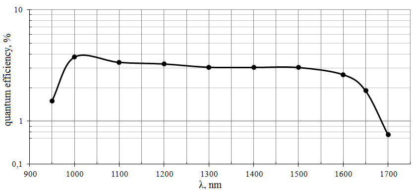
The photocathode, which operates in the NIR, also known as the transferred electron (TE) photocathode, can move the long-wavelength threshold of photoemission by increasing the internal energy of the photoelectrons. This structure has been realized on the basis of heteropair InP-InGaAs. Titanium grid-electrode (Schottky-barrier) was inflicted on the heterostructure surface. After that photocathode structure was purified by 2-step method (chemical cleaning and vacuum annealing) [4- 5]. Atomic clean InP/InGaAs surface activated with Cs and O2 allows to form effective state of negative electron affinity on photocathode surface [1-2,6]. In the real device backside bombarded technology is implemented. Photocathode structure is irradiated from the InP substrate to the emitter layer. The dependence between the quantum efficiency (QE) of the proposed InP/InGaAs heterostructure which works in transmission mod and is represented in figure 1. The photocathode demonstrates stable QE on the level of 3-4% in NIR. Such values of efficiency are enough to create sensor on the basis of developed heterostructures.

Fig1
4. Receiver of photoelectrons
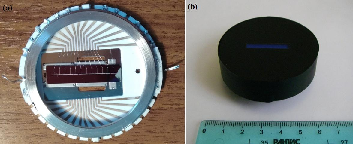
In the device layout with InP/InGaAs photocathode the line of silicon pin-diodes with the number of elements equal to 12 was selected as the receiver of the photoelectrons and the amplifying element. It is a vertical structure on the basis of pure high-resistance silicon obtained by zone melting methods. Special features of creation of pin-diode lines ensure them to work in the reverse bias mode. In this mode a full depletion of the high-resistance base occurs, which ensures drift transfer of the charge carriers. It allows to obtain a time of the signal record at the level of a few nanoseconds. Figure 2 shows the line of pin-diodes on the technical testing adapter and appearance of the device layout.
Our experiments showed that the impulse response front of the photodiode is equal to 1.1 ns. and the impulse response duration is equal to 1.9 ns. Amplification is achieved due to the occurrence in the solid-state element (diode structure) of a large number of charge carriers by the influence of high energy (several keV) electrons emitting from the photocathode.

Fig2
Besides the level of sensitivity and processing speed of sensor another important parameter of device exists. That factor is an equitability which demonstrates the level of sensitivity obtained on the different elements of the diode line compared to each other. Figure 5 shows sensitivity of fabricated sensor for all elements of diode line simultaneously. The unevenness of device reaches the value of more than 50% which is highly undesirable. It happens mainly because of the unevenness of the photocathode. The main reasons of it are no ideal conditions of chemical cleaning of the photocathode structure and large active area of the photocathode. It creates the additional difficulties when performing technological operations like vacuum annealing and photocathode activation.
上一篇: 石英抛光方法
下一篇: 晶圆干燥的基本原理和技术