SOLUTION-BASED coating methods for electronic-device applications are the focus of intense research efforts for many compelling reasons: reduced costs, improved performance, and new functionality, just to name a few. The breadth of applications for passive- and active-element solution-based coatings spans displays, lighting, solar cells, sensors, wireless devices for radio-frequency identification (RFID), and medical devices.1 Here, the term active refers to using the semiconducting nature of the material as its primary function in a device; for example, in diodes and transistors. Most solution-based coating products that have achieved large-volume manufacturing are confined to passive elements where the electrical conductivity and/or optical or mechanical property of the solution-coated layer are the key to their functionality. Some examples are patterned bus lines, anti-reflective films, planarization layers, and phosphor layers. Few examples of solution-coated active devices have achieved large-scale commercial production.
Solution Technology
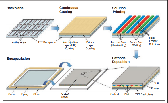
DuPont Displays has developed a low-cost AMOLED technology that combines highperformance OLED materials tuned for solution-processing, coating techniques, and methods optimized for OLED layers and the utilization of existing flat-panel-display equipment. This OLED fabrication process is outlined in Fig. 1, in which two solutioncoating methods are utilized: slot-coating for blanket layers and continuous nozzle printing for patterned layers. Figure 2 shows a vertical cross-section of an OLED device stack. The hole-injection layer (HIL) and hole-transport layer (HTL) are slot coated; the emissive red, green, and blue layers (EML) are nozzleprinted simultaneously, and a multi-layered cathode is blanket-evaporated. The brightness and color-uniformity specifications for flatpanel displays impose challenging thickness uniformity requirements for solution-coated OLED layers. The uniformity requirements are broken into several areas: long range (across the entire panel), short range (between neighboring pixels or inter-pixel), and within a subpixel (intra-pixel).
Figure 2 shows a schematic cross-section of high and low intra-pixel thickness uniformity and a corresponding example of a blue subpixel electroluminescent (EL) image. Interand intra-pixel thickness non-uniformity in the solution-coated layers can result in visual defects (mura) as well as non-optimal OLED device performance, and so our technical team developed several new analytical, metrology, and modeling methods to study and improve solution-coated layer uniformity.

Fig1
Slot-Die Coating is the preferred commercial solution-coating technique for preparing thin uniform blanket layers, and this technique has been scaled up to (at least) Gen 8 substrates for flat-panel-display processing. Slotdie coating is also being developed for use in general-lighting-based OLED applications.4 Figure 3 (top) shows optical profilometer data plotted as a contour map of our company’s HIL slot-die coated onto a 150 × 150-mm glass substrate. In this sample layer, we achieved, via slot coating, better than ±3% long-range layer thickness uniformity for a layer as thin as 600 Å.a.
We performed computational fluid-dynamic (CFD) modeling to better understand inertial spreading in nozzle printing. All CFD modeling used FLOW-3D, a volume of fluid simulation package from Flow Science, Inc., located in Santa Fe, New Mexico (www.flow3d.com). Figure 4 shows a sample CFD simulation output of axisymmetric impingement of a laminar jet on a surface. To verify the model’s ability to predict inertial spreading, we simulated hydraulic jumps, which have previously been well-described and pictured at larger length scales.9 We found no literature data for hydraulic jumps at lengths typical of our printing process, so we obtained jump radii (Rh) using the setup shown in Fig. 4. We obtained good agreement between CFD simulations and our experimental results.
上一篇: InGaP和GaAs在HCl中的湿蚀刻