A novel approach is presented for introducing a surface morphology with beneficial light scattering properties to sputter-deposited ZnO:Al films, which are used as front contact in Si thin film photovoltaic devices. Electrochemical anodization was used to trigger local dissolution, leading to interfacial structures complementary to those commonly prepared by an etching step in diluted HCl. By systematic variation of electrochemical etching conditions and electrolytes, the essential experimental parameters for designing the ZnO film surface were evaluated. The prepared films were characterized by scanning electron microscopy, four-point resistance and Hall measurements. Furthermore, electrochemical and chemical etching steps were combined to generate a diversity of different surface morphologies. The application of such films in microcrystalline Si single junction solar cells has shown promising initial results.
Silicon thin film solar cells require a highly transparent front contact with low series resistance. The most commonly applied transparent conductive oxide (TCO) materials for thin film solar cells are SnO2:In, SnO2:F, ZnO:Al, and ZnO:B,1 and the optimization of these TCO films has proven to be crucial for high cell efficiency.2 In superstrate configuration, the interface between the TCO and Si must provide a certain roughness for light scattering as to trap the light in the solar cell by total internal reflection within the absorber layer. For sputterdeposited ZnO:Al, this roughness is usually achieved in a chemical etching step with diluted HCl, resulting in the 'standard Jülich' material with a favorable surface morphology for light trapping issues.3 We have recently shown that diluted HF and mixtures of HF and HCl can be utilized to structure the ZnO film surface more selectively, which leads to a superior solar cell performance.4-6 For less compact ZnO films deposited at lower substrate temperatures, mild etching agents such as NH4Cl have to be utilized to achieve sufficient roughnesses.7,8 Even though the chemical etching of single crystalline ZnO has been thoroughly investigated in the 1960s9,10 on the basis of a dangling bond model,11 a significant complexity arises from the polycrystalline nature of sputter-deposited ZnO:Al thin films. Since the etch rate is strongly dependent on the crystalline orientation,10 an inhomogeneous etching occurs on structurally heterogeneous substrates leading to complex topographies as the material corrosion proceeds. This fundamental complexity requires a constant optimization of etching conditions according to the substrate material and therefore accounts for the ongoing efforts invested in this field.
Alternatively, electrochemical processes can be utilized to deposit or modify TCO materials for solar cell applications. The electrochemical deposition of TCO films has been applied for instance in the field of organic photovoltaics12 or the generation of template-based porous structures13-15 – with the mechanistical fundamentals being well understood.16-19 The beneficial effect of cathodically deposited back contact ZnO for the light trapping properties of Si thin film solar cells has been demonstrated20 as well as the electrochemical deposition of complete CuInSe2 thin film solar cells.
In this paper, a new approach is presented for introducing a unique surface morphology to sputter-deposited ZnO:Al films. Electrochemical anodization is used to trigger local dissolution of the material, leading to interfacial structures complementary to those of the standard Jülich ZnO prepared by simple chemical etching. The fundamental differences between chemical and electrochemical etching processes outlined in a recent work22 therefore allow for the introduction of novel surface structures. Unique morphologies with beneficial light scattering properties are prepared by combination of electrochemical and chemical etching steps and investigated in terms of their utilizability for microcrystalline Si (µc-Si:H) single junction solar cells.
ZnO:Al thin film deposition. Approximately 800 nm thick, polycrystalline ZnO:Al films were deposited on a cleaned (1010) cm2 glass substrate (Corning Eagle XG) using radio frequency (RF) magnetron sputtering in a vertical in-line system (VISS 300, VON ARDENNE Anlagentechnik GmbH, Dresden, Germany) from a ceramic target consisting of ZnO with 1 w/w% Al2O3 (Cerac Inc., Milwaukee, WI, USA). The deposition was carried out at a substrate temperature of 300°C, a discharge power density of 2 W cm-2, and an Ar pressure of 0.1 Pa. Details about the process have been published elsewhere.

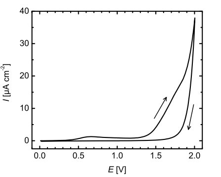
Independent of the corrosion mechanism, the anodic ZnO dissolution leads to a surface morphology where the grain boundaries deepen in the course of the experiment (Fig. 2). Obviously, both possible interfacial reactions (Eqs. 1 and 2) are distinctly limited to the grain boundaries of the polycrystalline material with a stunning degree of selectivity, and do not attack the ZnO grains. In case of RF-sputtered ZnO films, the crystallites preferentially grow toward the [0001] direction, which means that the grains are highly c-axis oriented after the deposition.35 This has also been observed for the ZnO films used in this study.36 Hence, the dissolution rate of the c-axis oriented grains under anodic polarization seems to be negligibly low, especially when compared to the dissolution rate at the grain boundaries. Surface profilometric measurements support that observation, as no integral thickness changes are observed after the electrochemical treatment. Thus, the resulting structure differs remarkably from the crater-like structures of the standard Jülich ZnO, which is etched in diluted HCl only.3,4 Even though the grain boundaries are also the origin of crater growth when etching with HCl, in particular the triple points of grain boundaries,37 the c-axis grains are always etched as well in this case. In contrast to electrochemical etching, the chemical etching is dominated by the diffusion of protons towards the surface.22 Consequently the resulting craters can extend even over several grains.
下一篇: 可选择性去除氧化铝的湿式蚀刻法