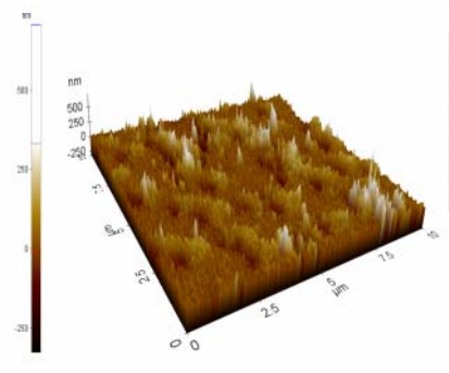
In this work, ultrasonically enhanced chemical etching was employed to fabricate porous silicon layer. Porous silicon layer was fabricated in p-type (111) orientation silicon by using HF solution, and HNO3. It was found the structure of porous silicon layer on p-type Si was improved by ultrasonic. Porous silicon micro cavities with much higher quality factors can be fabricated by this method. The improved quality induced by ultrasonic etching can be ascribed to increased rates of escape of hydrogen bubbles and other etched chemical species from the porous silicon pillars' surface. The effect is attributable to effective change in the concentration of free holes carriers. Ultrasound has led to indicating probably a change in bonding configuration, and increase in oxidation. Also, a correlation was established between the ultrasonic treatment and the microstructure.
Porous silicon (PS) is a new material which has attracted attention for use in silicon based optoelectronic devices. Efforts are going on worldwide to exploit its unique properties of visible photoluminescence (PL) and electroluminescence (EL) for new applications. An important property of PS, which needs to be studied in detail, is its high reactivity with chemicals due to its large surface area and surface defects. The surface area per unit volume in this material can range from a few m2 /cm3 to 200 m2 /cm3 , depending on the fabrication conditions. The surface can adsorb gases, liquids or chemical vapours, resulting in drastic changes in its properties.
Studies on PS properties for various applications have been undertaken by many researchers. The fact that efficient EL is observed when liquid contacts are used suggests that electrical properties are affected by the presence of liquids. Another interesting aspect is the remarkable electronic passivation of silicon surfaces achieved using various techniques. Very low values of surface recombination velocities have been achieved by simple immersion of bulk silicon in hydrogen fluoride (HP), leading to surface recombination centers < 108 cm-2. This has been ascribed mainly to complete hydrogen termination of surface with no dangling bonds.

Fig1
The chemical composition of the surface of the macro porous was investigated by means of the transmission spectra in the FTIR spectroscopy. The FTIR transmission spectrum on freshly prepared PS layer which prepared by chemical etching at different wavelength from 400 to 4000 cm-1 is shown in Figure-2.
The ultrasonic treatment during PS layer formation resulted in the Microstructural features in p-type (111) Si. As can be seen from this Figure, the freshly prepared PS layer showed Si-H absorption bands at 2400 cm-1. These modes are related to groups adsorbed at the extended PS surface. It is already well known that Si - Hx content is necessary for the passivation quality, as hydrogen may easily diffuse at the PS/Si interface as well as inside the Si wafer itself.
In summary, we have presented an ultrasonic enhanced chemical etching method for fabricating PS layer. Surface investigations atomic force microscopy (AFM) reveal that when other etching parameters are constant, the ultrasonic etching creates a thicker and more uniform PS layer, with smaller silicon pores than nonultrasound chemical etching.
AFM observations further confirm the improved structural properties, which can be explained by the PS formation mechanics, especially by ultrasonic cavitation. The studies of both PS single layer and PS micro cavity show that ultrasonic etching optimizes the sample’s characteristics. The best quality sample has been acquired by combining the ultrasonic etching with usually technique. This new etching method is very efficient technique to fabricate PS materials, especially PS multilayer, and opens a feasible way to realizing the application of PS materials.