Abstract—The fabrication of gallium-nitride based (GaN) light emitting diode (LED) arrays by a direct writing technique, itself using micron-sized LEDs (micro-LEDs), is reported. CMOSdriven ultraviolet GaN-based micro-LED arrays were used to pattern photoresist layers with feature sizes as small as 500nm. Chequerboard-type square LED array devices were then fabricated using such photoresist patterns based on either single pixel or multi-pixel direct writing, and implemented as part of a completely mask-less process flow. These exemplar arrays comprised either 450nm-emitting 199x199µm2 pixels on a 200µm pitch or 520nm-emitting 21x18µm2 pixels on a 23µm pitch. Fillfactors of 99% and 71.5% were achieved with optical output power densities per pixel of 5W/cm2 and 20W/cm2 at 90mA and 6mA dc injected currents, respectively.
We report here on the use of 8x8 micro-LED arrays with pixel sizes as small as 14µm-diameter in an imaging optical setup (similar to the setup in ref.but with a 10:1 demagnification) to pattern PR with features down to 500nmwidth in order to process GaN-based LED heterostructures. First, a single pixel was used to pattern a sacrificial PR mask for a “chequerboard-type” array with individually addressable LEDs emitting at 450nm.The chequerboard device was designed with a targeted 1µm gap between adjacent pixels, resulting in a 99% filling factor arrays in a suitable configuration for subsequent flip-chip bonding to custom complementary metal-oxide-semiconductor (CMOS). Typical measured optical output powers here were 2mW (5W/cm2 ) per pixel at a driving current of 90mA. Parallel direct writing is then implemented using 2 micropixels each of 24µm diameter to create a 32x32 chequerboard design emitting at 520nm. This had 21 x 18µm2 pixels on a 23µm pitch, each delivering 77µW (20W/cm2 ) at 6mA injection current. These arrays were fabricated in a suitable configuration for applications including lab-on-chip sensors, micro-displays, time-resolved spectroscopy and optoelectronic tweezing, and provide demanding demonstrations of the capabilities of micro-LED direct writing in the rapid and accurate fabrication of active optoelectronic devices.
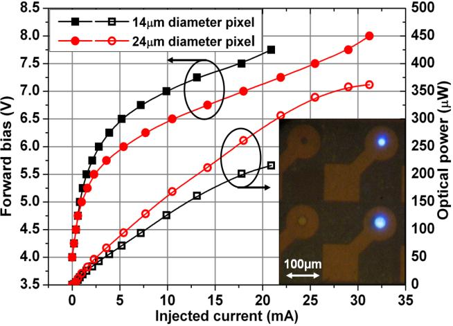
The parallel writing capability of our setup was then demonstrated with 2 adjacent 24µm-diameter pixels (namely pixels 7 and 8 from Fig. 2(a)) driven at the same forward bias voltage, 7.5V (25.5mA typical dc injected current). The pixels were both placed within the field of view of the collection microscope objective so that their emission is collected altogether. In this configuration and driven individually, each pixel delivers a different optical power at focus of 0.163µW (3.6W/cm2 ) and 0.17µW (3.75W/cm2 ), respectively, due to variation in pixel-to-pixel performances as shown in Fig. 2(a). However, due to the characteristics of the CMOS design, the current flowing through the chip when several LEDs are driven simultaneously induces a voltage drop at the LED electrodes due to the ground bounce effect.Consequently, when driven simultaneously, the optical power projected is not the sum of the individual optical powers, instead a total optical power at focus of 0.131µW (2.9W/cm2 ) is estimated per driven pixel. The chequerboard-design was again chosen to illustrate the lithographic capability in this case for high density micro-LED arrays emitting at 520nm. An array of 32 x 32 elements with a 23-µm pitch was thus coded for a 2 pixel writing experiment. In the vertical direction (direction according to inset of Fig. 4.) each trench is exposed using a single pixel while, in the horizontal direction, both pixels are used consecutively. The writing speed was fixed to 100µm/s in vertical giving a typical exposure dose of 69mJ/cm2 , and 200µm/s in the horizontal direction to take into account the overlapping exposure path from the two pixels. After PR patterning, the same etching process was applied as described previously resulting in an array of individually-addressable rectangular pixels. In this case the resulting fill-factor is reduced to 71.5% with 21x18µm2 pixels as shown in the optical micrograph inset of Fig. 4. Probes were used here to electrically and optically characterize the device. Fig. 4 summarizes the typical I-V and L-I curves for a pixel of the array. The pixel delivers an optical power of 77µW at an injection current of 6mA, giving an optical power density of 20W/cm2 with current density of 1.6kA/cm2 .

Fig1
A custom-made 370-nm emitting micro-LED array bonded on CMOS backplane was used as a maskless photolithography tool to fabricate complex and tailored optoelectronic devices through the use of an optical demagnifying setup and computer control. This direct writing technique was first used to pattern PR layers giving features as narrow as 500nm at 140µm/s writing velocities. In combination with wet and dry etching and inkjet printing, custom designed 450nm emitting, 99% fill factor, 8x8 broad-LED array and 520nm-emitting 32x32 micro-LED array were fabricated by single and two-pixels parallel writing respectively. Typical optical output powers emitted by a single element were measured to be up to 5W/cm2 and 20mW/cm2 , respectively, at injected current of 90mA and 6mA. These results demonstrate the advantages of micro-LED maskless lithography, including re-configurable written patterns with sub-micron feature sizes and multi-beam parallel writing and implementation as part of a mask-less process flow, to address the easy fabrication of complex optoelectronic and photonic devices such as, but not limited to, GaN-based LED arrays.
上一篇: 单晶片炉的设计及在快速热处理中的应用
下一篇: 使用 UV LED 的无掩模光刻