Impressive advances in the epitaxial growth of III-nitride compound semiconductors have recently been made. These semiconductors have been widely used in both electronic devices and optoelectronic devices. III-nitride compound semiconductors possess excellent properties that include wide band gap, high critical breakdown fifield, and high electron saturation velocity, which have encouraged the rapid development of III-nitride-based transistors over the past decade.However, the power-handling capability of these devices still suffers from the leakage current through the Schottky gate. Furthermore, the long-term thermal stability of Schottky contacts to III-nitride semiconductors has not yet been achieved at high temperatures. To reduce the gate leakage current, increase the high breakdown voltage, and operate more reliably at a high temperature, metal–oxide– semiconductor (MOS) or metal–insulator–semiconductor structures are being widely investigated. In previous reports, a number of gate dielectrics such as AlN,4 SiO2 , 5 Si3N4 , 6 Ta2O5 , 7 and Ga2O3 (Gd2O3) 8 have been used in the MOS structures. However, the grown external dielectric layers were contaminated by surface contaminants from the original semiconductor. Furthermore, the associated stoichometric structure was greatly inflfluenced by the growth conditions. Foreign contaminants of the Ga oxide/GaN structure can be avoided, if Ga oxide can be grown on GaN layer directly. In this research, a photoelectrochemical method utilizing a He–Cd laser was used to grow Ga oxide on n-type GaN and the performance of the resultant MOS varactor devices was demonstrated.
The epitaxial layers used in MOS devices were grown on c-plane (0001) sapphire substrates using a metalorganic chemical vapor deposition system. Trimethylgallium and ammonia were used as the Ga and the N sources, respectively. Silane was used as the Si source for the n-type dopant. An undoped GaN buffer layer, with a thickness of 800 nm, was grown on a sapphire substrate at 520 °C, followed by the growth of a 600 nm thick Si-doped GaN layer at 1050 °C. Using Hall measurements performed at room temperature, the electron concentration and mobility were found to be 3.223 1017 cm2 3 and 350 cm2/V s, respectively.
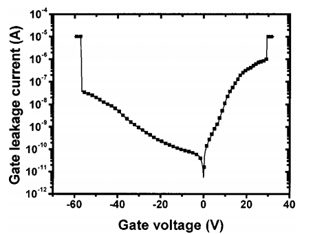
Figure 2 shows the current–voltage characteristics of the MOS devices measured by an HP4145B semiconductor parameter analyzer. It can be seen that the forward and reverse breakdown voltages are 28 V (corresponding breakdown fifield5 2.80 MV/cm) and 57 V (corresponding breakdown fifield5 5.70 MV/cm), respectively. The breakdown voltage is defifined as the voltage where a rapid increase of corresponding leakage current occurs. When a forward bias is applied, many electrons in the n-type GaN accumulate at the interface between the Ga2O3 layer and the n-type GaN. However, when a reverse bias is applied to the MOS device, few hole carriers will accumulate at the Ga2O3 /n-type GaN interface. Therefore, the reverse breakdown voltage is larger than the forward breakdown voltage. This carrier accumulation phenomena can also explain the fact that the reverse leakage current is smaller than the forward leakage current, as seen in Fig. 2.

Fig2
In summary, we report on the growth of a Ga2O3 layer directly on n-type GaN using a photoelectrochemical method by the application of a He–Cd laser. MOS devices were fabricated with the oxidized n-type GaN samples. The forward and reverse breakdown electric fifields of the grown Ga2O3 layer were 2.80 MV/cm and 5.70 MV/cm, respectively. The density of the interface states of the Ga2O3 /n-type GaN was 2.533 1011 cm2 2 eV2 1. An extremely low reverse leakage current of 200 pA operated at 2 20 V was achieved. We thussee that Ga2O3 layers grown by this photoelectrochemical oxidation method using He–Cd laser illumination are suitable for inversion layer formation. This MOS structure appears to be a promising candidate for applications of GaN metal–oxide–semiconductor fifield-effect transistors.
上一篇: 用于自旋电子学的宽带隙GaN基半导体
下一篇: 低温对湿蚀刻法制备微环谐振器的影响