An etching technique for the determination of the metallic impurities distribution in silicon wafers has been developedAn area of 10 mmo and 10 um depth was etched by 100 uL of an etching solution with a HF and HNO: mixture. Theacid matrix was evaporated on the wafer surface by lR lamp illumination and vacuum exhaust. Metallic impuritiesremaining on the wafer surface were redissolved into the collection solution, which was measured by electrothermaatomic absorption spectrometry (ET-AAS). The recovery invested by local etching/ET-AAS was within 95 - 112% foFe, Cu and Ni The detection limit (3) for Fe, Cu and Ni in silicon was 1 1013 atoms/cm To confirm theapplicability, local etching was applied to evaluate the effects of metallic impurities in a gettering study and the electronicproperties of semiconductor devices. lt was found that local etching is a useful sample preparation technique for theanalysis of metallic impurities in a specific area on a silicon wafer.
As the packing density increases in anultra-large-scaleintegrated(ULSI)device manufacturing process,therequirement of an acceptable metallic contamination levelbecomes more stringent! Because trace amounts of metallicimpurities affect the performance of electronic devices, a highlyprecise analytical technique is demanded.Vapor-phasedecomposition ( VPD) sample preparation is one of the mostprevalent analytical methods for metallic impurity analysis.Oxides on a silicon wafer are decomposed with HF vapor, ormixed acid vapor, and then a liquid droplet is rolled on thehydrophobic surface. WPD preparation has been coupled withseveral different trace elemental analytical techniques, such asinductively coupled plasma mass spectrometry (ICP-MS)4-7atomic absorption spectrometry (AAS)8- and total-reflectionX-ray fluorescence (TXRF)12-14.
In this paper, the analytical method for a specific area on awafer is described. For the sample preparation of a local areaand a specific depth of a silicon wafer, a sampling apparatus hasbeen developed. The etching area can be easily defined usingthis apparatus at the same fixed positions on several wafers.After preparation, Fe, Cu and Ni were measured by the ET-AAS. Determination by ICP-MS or ET-AAS is a commontechnique for the analysis of metallic impurities. Even thoughICP-MS has a lower detection limit, it needs a special sampleintroduction system for a small-volume sample containing Siand HF. Because of a few instrumental limitations, ET-AASwas used in this experiment. As an application using a localetching apparatus, wafers annealed after the contamination ofmetallic impurities and patterned wafers were analyzed.
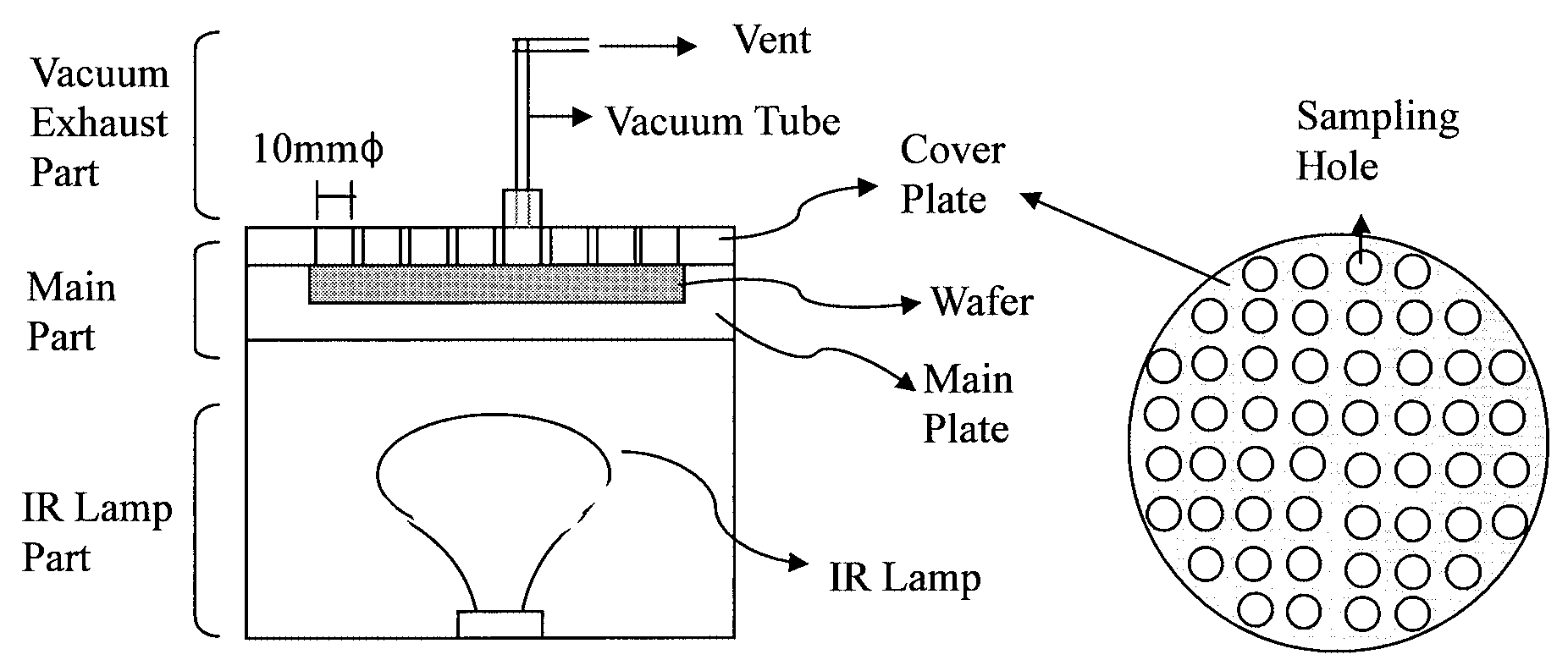
The apparatus is divided into three parts: main part, IR lamppart and vacuum exhausting part. The main part is composed ofa main plate and a cover plate with punched holes. Also, an IRlamp is set for heating the etching solution, and the reaction gasis ented by the vacuum exhausting part. The diameter of' thesampling tube is 10 mmo. The sampling tube is designedespecially for protecting the leakage of the etching solutionwhile the silicon wafer is being etched.

Fig1
A Perkin Elmer ZL5100 GF-AAS (Perkin Elmer, Norwalk.CT, USA) equipped with a Zeeman background corrector wasused to measure Fe, Cu and Ni. A pyrocoated graphite tube wasused, the operating conditions are described in Table 1. Forsample preparation, the etching apparatus is made withpolytetrafluoroethylene (PIFE).A schematic diagram of theetching apparatus is shown in Fig. 1.
A recovery test was carriedout at the optimal etchingconditions. One hundred microliters of a 1.0 ng mL-1standardsolution of Fe, Cu and Ni were pipetted onto the wafer surface.and dried by an IR lamp. The area containing a contaminatedspot was analyzed with a local etching technique. The recoverywas determined as the ratio of the measured concentration to theinitial contaminated concentration. A recovery of 95 - 112% was obtained from the mean of five samples, as tabulated inTable 3.
上一篇: 一种测量OLED材料介电强度的方法
下一篇: 不同层对OLED性能的影响