Organic light-emitting diode (OLEDs) displays are a promising new display technology that possesses advantages such as thinner and flexible displays, lower power consumption, and a wider viewing angle. The materials used in OLEDs produce a high fluorescence with a small voltage which makes them more efficient than current display technology. There are two main types of fabrication currently in use for OLED’s. The first, smallmolecule OLED technology, requires vacuum deposition and typically uses a glass substrate. The second, which utilizes a deposition technique derived from ink-jet printing can be applied to a variety of substrates including flexible ones. The use of flexible displays generates much interest in the consumer market because of the possibility of new applications. This paper will focus on some of the many different approaches to OLED fabrication as well as techniques involved in producing full color displays.
Electronics manufacturers are continuously investigating ways to minimize the cost of the devices they produce. In electronics containing a display, the cost to manufacture is in large part due to the display component. Because of this, much research is devoted to either improving existing displays or looking into new, alternative display technologies. Organic light emitting diodes (OLEDs) are one such technology.
The possible applications of this display technology are numerous. Because of their unique form and intrinsic characteristics, OLEDs can accomplish things current display technologies such as LCD and Plasma cannot. Obvious applications such as televisions and cell phone displays are currently being produced. Samsung has developed the largest OLED to date at 40 inches for a flat screen television as shown in Fig. 1.
More exotic applications that utilize flexible substrates are being investigated as well. Roll up displays are commonly referred to as the ‘break out’ application of OLEDs. When printing on a flexible substrate with an ink-jet method, it is conceivable one could produce a display that rolled up like a map or poster. This opens the door to further advances in portability of systems requiring a display such as laptops, televisions, or even video game systems.

Fig1
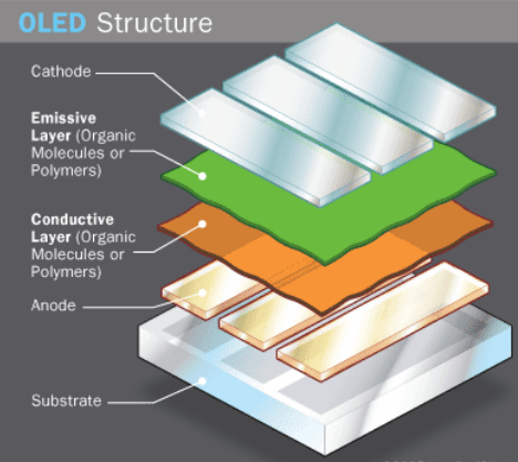
The organic layers can be made of either organic molecules or polymers. When using organic molecules two layers are used. One layer is called the transport layer and the other is called the emitting layer. The transport layer serves to pass electron ‘holes’ from the anode. The emitting layer passes electrons. When the holes and electrons interact an exciton is emitted and light is created. Many times the application will dictate the choice of layer material. One factor that will determine the material is the desired color.Different colors are achieved with different layer materials. For example, if green is desired it is common to use the combination Mq3 , where M is a Group III metal and q3 is 8-hydroxyquinolate. Blue is achieved by using Alq2OPh and red is done with perylene derivatives. When choosing a polymer, only a single organic layer is required.
When using small molecule layers, evaporative techniques are commonly chosen. The small molecules are evaporated onto a substrate and form a thin film. This takes place in a vacuum. Another method is called chemical vapor deposition (CVD). In CVD a substrate is placed in a vacuum and a chemical is introduced causing the film to condense onto the substrate. A disadvantage to this method is that everything inside the vacuum will get coated, leading to waste of material.
上一篇: 显示性能进展:AR、VR、OLED