In this paper we report on Cu plating of through-silicon-vias (TSV-s) using in-house made acidic Cu bath with model additives (SPS, PEG, and JGB). Although the model additives might not be as potent as commercial additives, they have been studied in detail, and their role in Cu plating has been described extensively in scientifific literature. This in turn allows deeper insight into how changes in bath composition affect the plating mechanism and Cu via-fifill.
Establishing a cost-effective technology for the metallization of through-silicon-vias is an important factor in the realization and volume manufacturing of 3D-stacked integrated circuits (3D-SIC). Cu electroplating should provide not only a void-free TSV fifill, but also short plating time and small overburden. The fifilling results depend on factors such as via dimensions, current density, current waveform, Cu bath composition, mass transport phenomena, and properties of the seed .
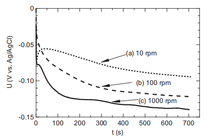
The plating experiments were performed using in-house made virgin make-up solution or VMS (aqueous acidic Cu-sulfate solution with Cl- ), and model additives such as poly-ethylene glycol (PEG), bis(3-sulfopropyl) disulfifide (SPS), and Janus Green B (JGB). Coupon-level experiments were performed using three-electrode rotating disk electrode (RDE) setup and computer controlled Autolab/Metrohm PGSTAT30 potentiostat. Working electrode (WE) was the coupon with TSV-s. The sample area (i.e. the apparent area of the WE) was 1.5 cm2 . The true area of the WE, including the area of TSV sidewalls, could be up to three times larger than the apparent area, depending on the via density. Deposition current density was calculated using the apparent WE area. A Pt mesh was used as a counter electrode (CE), and was separated from the WE by a diaphragm, which prevents anodic additive breakdown products from affecting the deposition process. Ag/AgCl was used as a reference electrode (RE). Volume of the electrolyte in the plating cell was between 100 and 300 ml. The same bath was used for plating of two coupons, and then replaced by a fresh Cu bath. The additive consumption was not monitored in coupon-level experiments.

Fig1
With the further increase in aspect ratio, the processing window narrowed even more. Initial attempts to fifill 5x 40 lm vias using the model chemistry and a single DC plating step within 1 h have failed. It was only after the requirement for plating time was relaxed that reasonably good Cu fifill was obtained. However, it took 2+ h to do so, which made us explore the use of pulse-reverse (PR) current waveforms for plating of higher aspect ratio vias. PR current waveform we used consisted of forward (deposition), reverse (stripping), and off (zero current) step. The PR waveform, which typically lasted a fraction of a second, was repeatedly applied until the via was fifilled. Current density and the duration of each step were tailored based on the characteristic feature dimension, and mass transport requirements for Cu ions and all the additives in the bath. More details on PR current waveforms can be found in [19–21] and references cited therein.
We have successfully fabricated Cu nails inside the vias with aspect ratios ranging from 2 to 8 (height/diameter), on both coupon- and wafer-level, using in-house made chemistry with model additives. We have demonstrated that the processing window narrows down with the increase in aspect ratio, and the transition from high-via-density (test-die-layouts) to low-via-density dielayouts. Good Cu fifill of 5 x40 lm vias required plating time between 1 and 1.5 h long and resulted in an overburden of approximately 3.5 lm. The limitations on the use of this chemistry for even higher aspect ratio vias, with smaller/larger via diameters, is yet to be determined from the analysis of the collected data, literature, and future experiments.
上一篇: 金属氧化物半导体电容器特性的表面处理
下一篇: CMOS晶圆加工工艺