The Texturization of crystalline silicon wafers by wet-chemical treatment is commonly used for the enhancement of light absorption in solar cells. Recent studies of anisotropic acidic etchants based on HF-HCl-Cl2 led to an innovative random inverted pyramid surface structure. By using the ‘wafer ray tracer’ of pvlighthouse.com.au the theoretical light absorption properties of the random inverted pyramid structure were compared to the well-known textures for PERC solar cells. We simulated pyramidal and inverted pyramidal structures with monomodal sizes and with various average pyramid widths. Besides, simulation of a PERC solar cell on the roof top (30°, south) of our building in Freiberg (N 50°55'32.16'', E 13°19'58.43'') on June 21st, 2016 (solstitium) was performed. The results encourage further development of new textures on monocrystalline silicon wafers by maskless acidic wet chemical treatment with HF-HCloxidant mixtures.
Theoretical discussions on the texture of monocrystalline silicon wafers have been made since the 1980s. These studies led to powerful Monte-Carlo simulation tools like OPAL 2 and the ‘wafer ray tracer’, which are based on assumptions of various ray paths and give the share of reflection, transmission and absorption of light for photogeneration of charge carriers.
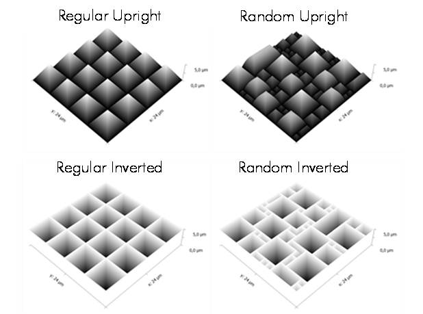
The goal of the present study was to identify ideal textures for a PERC solar cell. We examined four different types of surface structures on monocrystalline silicon wafers. Random inverted pyramid structures, recently found by HF-HCl-Cl2-treatment, are compared to the well-known types of surface structures on monocrystalline silicon wafers: regular upright, random upright and regular inverted (Figure 1).
For preparing the etching mixtures hydrochloric acid (37 wt%, analytical grade, VWR), hydrofluoric acid (48 wt%, analytical grade, Sigma-Aldrich) and deionized (DI) water were mixed in a PFA beaker. Dried gaseous chlorine was bubbled into the etching solution. Silicon wafer pieces of approximately 1 cm x 1 cm ((100) orientation, boron doped, thickness of 190 μm, resistivity of 0.5 − 2.0 Ω cm−1, Deutsche Solar GmbH, Freiberg, Germany) were placed with tweezers for 20 minutes in 30 mL of the etching mixture.

Fig1
The simulations were performed with the ‘wafer ray tracer’ of pvlighthouse.com.au. Parameters like wafer thickness, front and rear films were kept constant. Surface morphologies were varied as shown in Figure 1. Parameters for the Zenith and Azimuth were used from www.suncalc.org. The given values for absorption and reflectivity are average values for the wavelengths between 300 nm and 1200 nm.
Using HF-HCl-Cl2 mixtures for treatment of monocrystalline silicon wafers, random inverted pyramidal structures are generated without masking or lithographic processes. Silicon etching rates up to 0.35 µm min-1 are observed during etching of monocrystalline, diamond wire-sawn wafers at room temperature. SEM pictures show pyramid edge widths between 2 and 20 µm (Figure 3). On the Inside of the inverted pyramids a microstructure is observed.
下一篇: 催化剂浓度对硅金属辅助化学蚀刻的作用