Recently, wafer-level packaging (WLP) has become one of the promising packaging technologies due to its advantages, such as fewer processing steps, lower cost, and enhanced device performance compared to conventional single-chip packaging. Many developments on new WLP design, material, and process have been accomplished according to performance and reliability requirement of the devices to be packaged . For a lower cost, higher performance, and environmentally green packaging process, anisotropic conductive fifilm (ACF) flflip chip assembly has been widely used, such as in ultrafifine-pitch flflat panel display (FPD) and general semiconductor packaging applications, too. However, there has been no previous attempt on the wafer-level flflip chip assembly using ACFs. In this paper, wafer-level flflip chip packages using preapplied ACFs were investigated. After ACF prelamination on an electroplated Au bumped wafer, and subsequent singulation, singulated chips were flflip-chip assembled on an organic substrate using a thermocompression bonding method. Au-plated bumps were well assembled on Ni/Au pads of organic substrates. The electrical, mechanical properties and the reliabilities of wafer-level flflip chip assemblies (WL-FCAs) were evaluated and compared with conventional ACF flflip chip assemblies using the thermocompression method. Contact resistance measurement was performed after thermal cycling, high temperature/humidity, and pressure cooker test. ACF joints between electroplated Au bumps and substrate metal pads showed stable contact resistance of 5 m per a bump, strong bump adhesion, and similar reliability behaviors compared with conventional ACF flflip chip joints using a thermocompression bonding. As a summary, new wafer-level packages using preapplied ACFs were successfully demonstrated for flflip chip assembly. The new wafer-level packages using preapplied ACFs can be widely used for many nonsolder flflip chip assembly applications such as chip-on-board (COB), chip-on-flflex (COF), and chip-on-glass (COG).
Flip chip assembly has been widely used to mount IC chips to various substrates. In general, it is divided into two categories; solder bump flflip chip and nonsolder flflip chip according to their bump materials and assembly methods. Recently, WLPs using solder bumps have been already reported at various commercial applications using underfifill materials However, solder bump flflip chip has a drawback of bumping and assembly process complexity and higher production cost, because it requires a number of processes such as solder flflux coating, solder bump reflflowing, flflux cleaning, and underfifill dispensing and curing.
Currently, anisotropic conductive fifilms (ACFs) have been widely used in flflat panel display (FPD) packaging applications, such as a liquid crystal displays (LCDs) and a plasma display panel (PDPs) in forms of chip-on-board (COB), chip-on-glass (COG), and chip-on-flflex (COF). And ACFs are also extensively used at general semiconductor packaging applications with low power and have the potentials for high I/O devices. Comparing with solder bump flflip chip, nonsolder bump flflip chips assembled with ACFs have many advantages such as lower processing temperature, environment-friendly processes with no flflux and solders, fewer assembly steps, and fifine-pitch handling capability. However, there has been no previous attempt using ACFs on wafer-level packages.

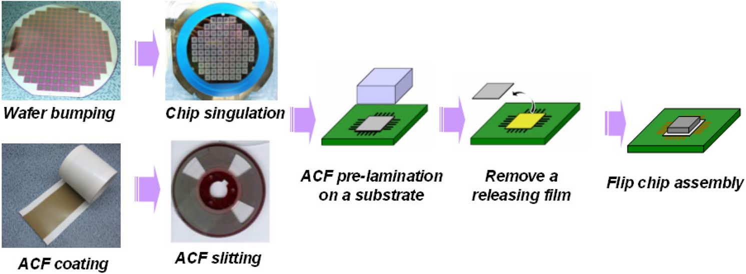
Fig1
At the fifirst step, ACFs are laminated on an entire wafer with nonsolder bumps without voids or bubbles formation. At this stage, ACFs should be maintained at the B-stage before curing, because partially cured ACFs may result in deterioration of bump contact resistance and reliability of assembled flflip chip joints. In the next step, an ACF-laminated wafer is diced into individual dies using a conventional diamond blade dicing saw. ACF delamination and silicon chipping may occur during the wafer dicing process because a B-stage ACF is much softer than silicon. Therefore, it is important to avoid ACF delamination and silicon fragmental residues on the ACF surface during the wafer dicing process. In addition, moisture absorption control is also important to maintain the reliability of flflip chip assembly because of the reported moisture-related ACF failure mechanism. Consequently, the fabrication process of WLP using ACFs should be optimized by modifying ACF lamination, wafer dicing, moisture drying conditions, and so on. Drying conditions are determined at the condition of complete removal of absorbed moisture without additional ACF curing.