Photonic integrated circuits (PICs) enable the miniaturizing of complex quantum optical circuits with large numbers of photonic devices connected with optimized insertion losses and phase stability. Photons in a PIC are routed in a single spatial mode of a low-loss single mode waveguide, consisting of a high index core surrounded by lower index cladding materials to provide confifinement of the optical mode. Spatial mode matching, which is crucial for classical and quantum interference, can be nearly perfect for such an architecture. The use of PICs moreover allows integration of several functionalities on a single chip, including photonic cavities to enhance light-matter interaction, fifilters to block or select specifific wavelengths, integrated photodetectors, etc. A central building block for such quantum photonic circuits are single photon emitters (SPEs). Over the past decade a variety of material systems have been investigated to create on-chip SPEs, including III–V quantum dots, carbon nanotubes, GaSe crystals, and crystal colour centers such as the NV6 or SiV centers in diamond.
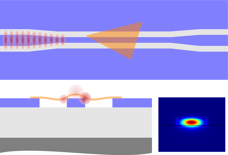
To maximize the count rate of an integrated single photon source, the fraction ηwg of total PL that couples to the waveguide mode should be as close as possible to one. It is, however, impossible to achieve this with the simple waveguide geometry shown in Fig. 1a, but interaction with a cavity can signifificantly boost the overall coupling rate to the guided mode. As an extension of our experimental results we will therefore investigate for which cavity parameters near-unity waveguide extraction effificiencies can be obtained. An essential parameter in this calculation is the cavity-emitter coupling, which critically depends on the dipole moment strength of the integrated 2Dbased emitter. For realistic estimates of this value, we will assess it from our experiments. As such we can get a clear overview of which cavity Q–factors and mode volumes Vc are required to maximize single photon extraction.
Here we study the integration of a WSe2 monolayer onto a SiN chip and demonstrate the coupling of 2D-based single photon sources with the guided mode of a SiN waveguide. We discuss how integrated cavity-emitter systems, evanescently coupled to a waveguide, should be designed to optimize single photon extraction into the waveguide. As such the full potential of a high quality and CMOS-compatible PIC platform can be exploited without the need for stringent processing in the host material itself. In combination with wafer-scale growth of 2D materials, this provides a promising route towards scaling of quantum photonic circuits.

Fig1
Waveguide-coupled single photon source. We will now focus on spot S5 of Fig. 2a and investigate the quantum nature of the observed emitters in more detail. The confocal and waveguidecoupled spectrum of spot S5 are shown in Fig. 3a. We observe a few peaks recurring in both the confocal and waveguide spectrum, confifirming that these emitters are indeed coupled to the waveguide. A prominent and isolated waveguide-coupled peak (FWHM ≈3 meV) appears around 1.64 eV (756.5 nm). It has been shown that the PL of 2D-based quantum dots can be enhanced when the excitation laser wavelength is tuned close to the free excitonic resonance9. When we scan the excitation wavelength with a tunable Ti:saph laser around the free exciton wavelength, we also fifind a considerable increase in peak count rate and reduction in background compared to excitation with λ = 532 nm for the same excitation power (see inset Fig. 3a). An excitation wavelength of λ = 702 nm provided the most optimal ratio between peak count rate and background, and hence the emitter was pumped at this wavelength for all subsequent experiments.
In conclusion we have demonstrated that integration of a WSe2 monolayer onto a SiN waveguide results in quantum emitters evanescently coupled to the waveguide. Second-order correlation measurements on a spectrally isolated quantum emitter confifirm that single photons are emitted with a waveguide-coupled saturation count rate of 100 kHz. These results confifirm previous claims that strain-induced quantum emitters could be coupled to photonic structures. A numerical analysis on the optimization of single photon extraction and indistinguishability using integrated dielectric cavity-emitter systems indicates that near-unity single photon extraction can be achieved, even for low quantum yield emitters. The presented approach for integration of strain-induced TMDC-based SPEs retains the favorable attributes of SiN PICs without the need for stringent processing in the quantum emitter host material itself. Recent progress in wafer-scale growth and patterning of identical 2D-material based devicesprovides a promising route in combination with our waveguide-coupled 2DSPEs to scale up quantum photonic circuits.
上一篇: 控制和改进KOH蚀刻的方法