The light output of deep ultraviolet (UV-C) AlGaN light-emitting diodes (LEDs) is limited due to their poor light extraction efficiency (LEE). To improve the LEE of AlGaN LEDs, we developed a fabrication technology to process AlGaN LEDs grown on SiC into thinfilm flip-chip LEDs (TFFC LEDs) with high LEE. This process transfers the AlGaN LED epi onto a new substrate by wafer-to-wafer bonding, and by removing the absorbing SiC substrate with a highly selective SF6 plasma etch that stops at the AlN buffer layer. We optimized the inductively coupled plasma (ICP) SF6 etch parametersto develop a substrateremoval process with high reliability and precise epitaxial control, without creating micromasking defects or degrading the health of the plasma etching system. The SiC etch rate by SF6 plasma was ~46 µm/hr at a high RF bias (400 W), and ~7 µm/hr at a low RF bias (49 W) with very high etch selectivity between SiC and AlN. The high SF6 etch selectivity between SiC and AlN was essential for removing the SiC substrate and exposing a pristine, smooth AlN surface. We demonstrated the epi-transfer process by fabricating high light extraction TFFC LEDs from AlGaN LEDs grown on SiC. To further enhance the light extraction, the exposed N-face AlN was anisotropically etched in dilute KOH. The LEE of the AlGaN LED improved by ~3X after KOH roughening at room temperature. This AlGaN TFFC LED process establishes a viable path to high external quantum efficiency (EQE) and power conversion efficiency (PCE) UV-C LEDs.
AlGaN ultraviolet light-emitting diodes (UV LEDs) and ultraviolet laser diodes (UV LDs) in the range of 265–280 nm are needed to develop novel disinfection and sterilizing technologies (water, air, and surfaces) to improve access to clean water , improve public health , and enable other biotech applications . UV LEDs are a viable technology for replacing mercury gas discharge lamps in disinfection and biotechnology applications . Hospitals, for example, reduced the rates of hospital-acquired drugresistant infections by 25% using ultraviolet disinfection (via mercury lamps (254 nm)), as reported by various clinical trials . Furthermore, the AlN or AlGaN epi-transfer and heterogeneous integration technology can be employed to enhance the performance of photodiodes (PDs) , high electron mobility transistors (HEMTs) , bulk acoustic resonators (BARs) , and high-aspect-ratio SiC microstructures and devices .
The most commonly employed substrates for AlGaN UV-C LEDs are sapphire and AlN but they yield LEDs with low LEE. Although sapphire substrates are transparent, their thermal conductivity is limited, and they lack efficient ways to extract TM polarization because roughening the sidewalls of sapphire LEDs dies is challenging . AlN substrates grown by physical vapor transport (PVT) are limited by an absorption around 264 nm (4.7 eV) with an absorption coefficient of about ~35 cm-1 whereas hydride vapor phase epitaxy (HVPE) grown AlN substrates have less absorption (~10 cm- 1 ) . Researchers have largely overlooked AlGaN LEDs grown on SiC substrates because SiC absorbs strongly below its optical bandgap (3.2 eV and 3.0 eV for 4H-SiC and 6H-SiC, respectively), but this disadvantage can be overcome with a novel thin-film flip-chip (TFFC) LED architecture in which the SiC is removed with a highly selective SF6 chemical plasma etch between SiC and AlN.

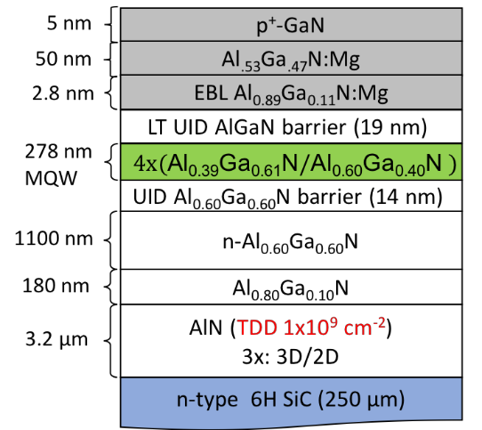
Fig1
We developed a highly selective SF6 plasma etch of SiC over AlN and a viable manufacturing method for epitaxial transfer from SiC to another substrate via wafer bonding and SiC substrate-removal by SF6 etching. Then, we demonstrated it on UV-C LEDs that were grown on SiC to fabricate high LEE TFFC LEDs. The SiC substrate was bonded via Au-Au thermocompression bonding to another n- and p-patterned thermally conductive substrate. The growth substrate was removed by a two-step ICP etching without micromasking defects on the etched surface. The first step was a high SiC etch rate (~46 μm/hr) at a high RF bias power (400 W). The second step was a selective SiC etch rate (~7 μm/hr) at a low RF bias power ( 49 W), with an etch selectivity of SiC:AlN ~90:1 at a process pressure of 1.33 Pa; higher SiC:AlN etch selectivity of ~150:1 was also achieved at a lower process pressure. The highly selective SF6 etch at low bias was essential for removing all SiC by reliably stopping at the LEDs’ AlN buffer layer, which acts as an etch stop layer. We demonstrated a TFFC manufacturing method for UV-C LEDs that were grown on SiC. The LEE was significantly enhanced via KOH roughening of the exposed N-face AlN. KOH roughening enhanced the LEE by ~3X for UV LEDs without encapsulation and despite the use of 5 nm p-GaN as a p-contact layer.
上一篇: 催化剂浓度对硅金属辅助化学蚀刻的作用