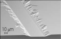
The technological aspects of manufacturing three dimensional microstructures for BioMEMS in glass wafers are demonstrated and discussed. The microchannels have been etched in Pyrex glass to a depth of 6–16 lm. Special attention has been paid to the composition and the optimization of the deposition process of the thin fifilm sacrifificial metal layers as etch masks for chemical wet etching of glass, and to the inflfluence of the composition of the etch solution on glass etch velocity, undercut phenomenon and the quality of the structures. The structures have been visualized by means of REM to observe the profifile and the edge roughness.
Initially, the fifirst microdevices were fabricated using silicon, but the technologies for manufacturing micro- flfluidic channels are being adapted to prepare the devices in other materials, such as glass and polymers (PDMS, COP). In comparison with silicon, these materials are advantageous for the on-chip CE application with regard to their electrical properties and optical transparency, which facilitates on-line optical detection. However, numerous problems dealing with the manufacturing issues of these devices are still remaining. In particularly, chemical wet etching of glass is often involved in wafer processing. Here, the composition of the etch mask and its adhesion to the glass surface during glass etching are most critical factors, which inflfluence the quality of the produced microstructures.
Mainly, two types of hard etch masks have been employed for an HF-based glass etch process. One of the etch mask system is Cr/Au (typically 20–40/150–200 nm). Better results have been achieved when using sputtering as the method of deposition of the metal etch masks. Sputtered thin fifilms were reported to have better performance as etch masks due to their high fifilm density and better adhesion, which prevents the etchant diffusion along the metal fifilm/ glass interface. However, sputtering is not always an available technique, the capital equipment for sputtering and the changes in the source material are expensive. Moreover, when using sputtering, the incorporation of impurities in the fifilm is possible. Another etch mask system is an amorphous silicon mask with a typical thickness of 100–200 nm. Using photoresist SU 8 as an etch mask for some wet-etching processes was also reported.
With regard to the glass etch mixtures used, we did not observe the difference in the quality of the resulted structures, when using a Cr/Au etch mask. In contrast, in the case of the Ni/Au system, nitric acid should not be used in the glass etch mixture because the nickel fifilm will be dissolved. With regard to the edge roughness and the absence of the pinholes, the best results were obtained, when employing 60 s Ar+ sputtering prior to the evaporation of the etch mask, Ni/Au (10–15/200 nm) etch mask system, and a slowly stirred 14.8% HF solution as a glass etch.

Fig1
The technological aspects of manufacturing 3-D microstructures in the Pyrex glass wafers have been discussed. The composition and the deposition technique (e-beam evaporation) of the thin fifilm metal layers as etch masks for chemical wet etching of glass have been optimized. The inflfluence of the composition of the etch solution on glass etch velocity, undercut phenomenon and the quality of the structures has been studied. It was shown that using the evaporated metal etch masks allows fabricating the structures, which are comparable with those prepared when using sputtered metal fifilms as a sacrifificial layers in glass etch process.