Josephson junction logic cells and superconductor microstrip lines are able to process and transfer digital data with ratesup to several hundred GHz as has been demonstrated in singlechip experiments. However, the existing chip-level bumping tech.nique in InSn solder and resulting inter-chip connections do notallow expanding these rates to multi-chip circuits. We developeda wafer-level bumping technology using lithographically-definedbumps deposited either by e-beam evaporation or electroplating.and proposed and implemented a novel design of high-frequencychip interconnects. Chip-to-chip single-flux-quantum pulse transmission rates reaching 110 GHz have been achieved. The observedrates were limited not by the interconnects but by the speed ofon-chip test circuitry fabricated in the framework of 4.5 kA/cmHYPRES process for superconductor integrated circuits. Experimental results on adhesive-bonded and reflow-bonded multi-chipmodules (CMs) with Au and InSn bumps are presented, and effective parameters of the new interconnect design and MC technology are discussed.
In this work, instead of manual chip bumping, we devel-oped a whole wafer bumping technology using lithographi-cally-defined bumps deposited either by e-beam evaporationor electroplating. This provides a 100-fold increase in theprocess throughput and over a 50-fold increase in the bumpuniformity as well as enables getting practically any desiredheight, diameter, and number of the bumps. We also proposeda novel design of interconnects which allowed us to achievechip-to-chip data transfer rates in excess of 110 GHz in theframeworks of HYPRES 4.5 kA/cm^ fabrication technology.
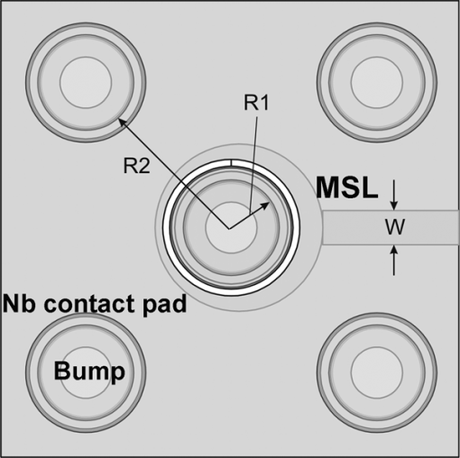
The usual arrangement of signal and ground contacts forchip-to-chip communication is a peripheral array shown inFig. 1. Each signal contact is surrounded by four ground con-tacts which can also be shared with the next signal contact.The signal (data) is coming along a microstrip line (width w)formed in one of the superconducting layers and marked MSLin Fig. 1. The bumps are formed in the centers of the signaland ground contact pads. Their diameter is somewhat smallerthat the diameter of the contact pads. The MSL impedance ismatched to a load or a driver at the other end of the MSL .

Fig1
Yet another advantage of the proposed design is that thesignal contact pad, although containing the ground plane layer.is isolated from the circuit ground in the x - y plane by a moatrather than by the interlayer dielectric in the 2-direction as iscommon to many conventional designs. This makes it possibleto apply significant pressure to the bump during flip-chipbonding without punching through the insulation and shortingthe signal bump to the ground. Also the distributed capacitancecan be varied independently of the size of contact pads andbumps.