Given the exceptional characteristics of diamond fifilms, they have become increasingly popular in the fifields of medicine, microelectronics, and detector electronics. However, despite all the advantages, there are many technological problems that complicate their widespread application and impose limitations on diamond use in technological processes. In this study, we proposed a new technique for obtaining a complex topology of polycrystalline diamond coatings by selective seeding of the substrate by nucleation centers and subsequent surface treatment with reactive ion etching to reduce the number of parasitic particles. As a result, diamond fifilms were obtained with a high particle concentration in the fifilm region and high repeatability of the pattern. Moreover, parasitic particles inflfluenced neutralization in areas where fifilm coverage was not needed. The effect of the diamond nanoparticle concentration in a photoresist and the effect of reactive ion etching on the formation of a continuous fifilm and the removal of parasitic nucleation centers were examined. The relative simplicity, low power consumption, and high effificiency of this method make it attractive for both industrial and scientifific applications.
Diamond coatings need to be deposited with high accuracy, but with minimal impact on adjacent layers. The optimal method will be able to obtain coatings with a predetermined pattern by using minimal processing/removal operations and a minimal inflfluence on any adjacent layers.
In previous works, we considered a technique for obtaining such coatings by the selective seeding of the substrate with diamond nanoparticles and the subsequent growth of the fifilm on this basis and no more surface treatments have been carried out. The nanodiamond nucleation centers remain due to Van-der-Waals forces and defects on the surface. This occurs during the plate preparation and application of a photoresist pattern with the addition of diamond nanoparticles. The presence of these particles causes the creation of parasitic nucleation centers for the future growth of diamond in the areas where the fifilms should not grow. Therefore, in areas that do not require diamond growth, islets and grains of the diamond are formed, which is highly undesirable, since such inclusions negatively affect the resolution of the pattern and the subsequent characteristics and the potential for uses of the fifilms. It is clear that a higher concentration of nanoparticles in the photoresist leads to the formation of a continuous fifilm earlier, but the resolution of the whole pattern decreases accordingly. Moreover, one of the important factors in the use of any technique is its processability, a shorter deposition time and a stable result plays an important role in determining the technology that will be used later.
In this study, we propose a new technique for obtaining a topology of polycrystalline diamond coatings using the technology of substrate selective seeding by the nucleation centers and subsequent surface treatment with reactive ion etching to reduce the number of parasitic particles.
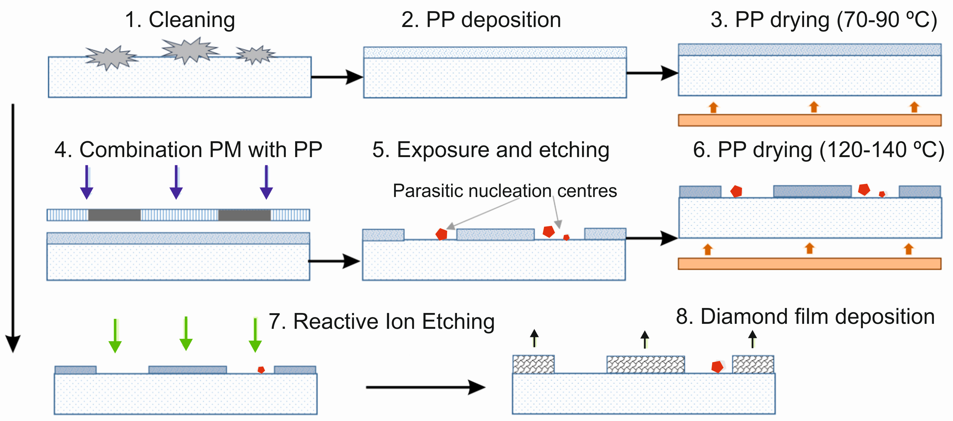
The silicon plates were then dried in a thermo-cupboard at a temperature of 70–90 ℃ to set the photoresist. The substrates were aligned with photomask (PM) followed by layer (AMK 2104.16, SORENG, St. Petersburg, Russia) by UV with λ = 250–440 nm. The photo layer was developed in an alkaline solution of KOH. Furthermore, the photoresist layer was additionally exposed to plasma etching in a nitrogen atmosphere. At the fifinal stage, the resulting silicon wafer was dried in a thermo-cupboard at a temperature of 120–140 ◦C (Figure 1). To remove parasitic nanodiamond particles, the substrate was subjected to reactive ion etching.

Fig1
The current density of the ion beam was 1.25 mA/cm2 with an energy of 3.3 ± 0.01 keV. Subsequently, the substrate surface was etched in a time range from 30 s to 30 min (Figure 2a). The current was set automatically with the power setting and could vary from changes in chamber pressure, gas flflow jumps, etc. The substrate temperature during etching was maintained at 23 ± 2℃ using an IR thermal imager (ULIRvision TI170, Zhejiang ULIRVISION Technology Co., Ltd., Zhejiang, China). After the etching process, the chamber was blown away from residual etch particles for 5 min with the same parameters. As a result of ion etching, we obtained regions consisting of an etched photoresist enriched with nanodiamond particles and a region free of parasitic particles.
下一篇: 光子晶体对LED光提取效率的影响