The global LED (light emitting diode) market reached 5 billion dollors in 2008 and will be driven towards 9 billion dollors by 2011. The current applications are dominated by portable device backlighting, e.g. cell phones, PDAs, GPS, laptop etc. In order to open the general lighting market doors the luminous effifi- ciency needs to be improved signifificantly. Photonic crystal (PhC) structures in LEDs have been demonstrated to enhance light extraction effificiency on the wafer level by researchers . However, there is still a great challenge to fabricate PhC structures on LED wafers cost-effectively. Nanoimprint lithography (NIL) has attracted considerable attentions in this fifield due to its high resolution, high throughput and low cost of ownership (CoO). However, the current NIL techniques with rigid stamps rely strongly on the substrate flflatness and the production atmosphere. Those factors hinder the integration of NIL into high volume production lines. UV-NIL with flflexible stamps, e.g. PDMS stamps, allows the large-area imprint in a single step and is less-sensitive to the production atmosphere. However, the resolution is normally limited due to stamp distortion caused by imprint pressure.
A novel NIL technique developed by Philips Research and Süss MicroTec, substrate conformal imprint lithography (SCIL), bridges the gap between UV-NIL with rigid stamp for best resolution and soft stamp for large-area patterning. Based on a cost-effective upgrade on Süss mask aligner, the capability can be enhanced to nanoimprint with resolution of down to sub-10 nm on an up to 6 inch area without affecting the established conventional optical lithographic processes on the machine. Benefifit from the exposure unit on the mask aligners, the SCIL process is now extended with UV-curing option, which can help to improve the throughput dramatically. In this paper, the fabrication of photonic crystal structures with SCIL technique on Süss MA6 mask aligner is demonstrated. In addition, the industrialization considerations of UV-SCIL process in high volume manufacturing are brieflfly discussed.
The global LED (light emitting diode) market reached 5.5 billion dollars in 2008 and is dominated by portable device backlighting applications e.g. mobil phones, PDAs, GPS, Laptop, etc. Emerging applications including general lighting will drive the market towards 9 billion dollars by 2011, according to Yole development report. However, the luminous effificiency needs to be improved signifificantly in order to open the market for LEDs to replace traditional light bulbs. Photonic crystal (PhC) structures in LEDs have been demonstrated to enhance light emission effificiency by diffractive waveguide structures. It is still a great challenge to fabricate PhC structures on LED wafers cost-effectively.
Substrate Conformal Imprint Lithography (SCIL), a novel NIL technique developed by Philips Research and Süss MicroTec, bridges the gap between UV-NIL using rigid stamps for best resolution and soft stamps for large-area patterning. Based on a costeffective upgrade on Süss mask aligner, the aligner capability can be enhanced to nanoimprint with sub-50 nm resolution up to 6 inch diameter area without affecting the established conventional optical lithographic processes on the machine. In this paper, the process details of SCIL technology and the imprint tooling are brieflfly described. Additionally, the introduction of SCIL into high volume manufacturing of high brightness LED (HB LED) is discussed.

Fig1
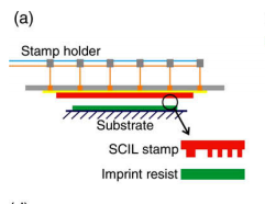
Although the PDMS stamp can compensate the waviness of the substrate, directly contacting a large-area stamp during replication can lead to non-conformal imprint or ‘‘bubbles” in case of using perpendicular imprint process. To achieve a substrate conformal contact between working stamp and substrate, the SCIL process relies on a sequential imprinting process where capillary forces help to pull the stamp into the liquid imprint resist. The approaching of the flflexible stamp starts from one side and spreads to the whole stamp subsequently by releasing the vacuum in the grooves step by step and applying an small over pressure of 20 mBar on the stamp. (Fig. 2a–c). This sequent contact mechanism prevents the flflexible stamp from trapping air and therefore ensures that the stamp follows exactly the undulating topography over whole substrate surface. The imprint resists that are used wet the PDMS stamp surface and the resulting capillary forces fifill up features with resists. The capillary forces are leading to minimized structure deformation and lateral stamp distortion during the imprint process. In this way sub-50 nm resolution patterns have already been demonstrated. After conformal contact over the entire substrate is carried out, the imprint resist layer is cured by UV exposure or in case of using imprint sol–gel based resists diffusion of the sol–gel solvent into the PDMS stamp . As the PDMS layer is ~ 5 mm thick compared to a resist layer thickness of 100 nm solvents do not saturate or swell the stamp. Additionally, solvents diffuse out of the PDMS on stamp release. The automatic separation of the stamp from the substrate is performed by switching on the vacuum in the grooves consequently, which is opposite to the imprint process (Fig. 2d–f). This results in a low force peeling action which removes the stamp from the patterned resist layer and avoids damage to stamp or patterns.
The 2D PhC structures for the HB LED wafers are desired to be hole arrays, which requires an array of protruding structures on the working stamp and therefore hole arrays on the master template. This makes the master fabrication with electron-beamlithography or laser interference lithography quite comfortable since complicated lift-off processes can be avoided, which can lower the fabrication cost as well. In addition, the 2D protrusions array on the working stamp is very process-friendly during mastering due to its uniform structure density distribution.