This study is concerned with the deformation or warping behavior of thin layered semiconductor structure comprising a silicon substrate, a pattern layer and a polyimide coating layer with its thickness varying from 100um to 50 um. In contrast with the conventional thick semiconductor structure, today’s semiconductor structure is increasingly thin and therefore the warping is extremely conspicuous, being among the major concerns in the structural design of a chip. In the view of thermomechanical analysis of an extremely thin layer structure considered in the present paper, a few parameters on the deformation should be taken into consideration such as the pattern layer and intrinsic stress. To account for the effect of the pattern layer, we make a well educated guess for the mechanical properties, employing the test results and the CBA (Composite Beam Analysis) theory. In addition, we take into consideration the effect of the intrinsic stress due to moisture absorption on deformation. We show that the chip warpage is accurately predicted when all these are properly considered. Furthermore, we have found that the local instability or wrinkling, associated with the nonuniformity or the inhomogeneity in material properties and bonding quality between any two neighboring layers, appears as one important mode of energy relaxation in addition to the overall warpage when the chip thickness becomes very small.
Memory package products are becoming increasingly thinner and multi-functional for the application of mobile microelectronics. Stacking techniques of multiple semiconductor chips inside a thin package are now among the essential parts of today’s advanced packaging technologies. For stacking a greater number of chips, the chip thickness has to be thinner, but this induces adverse effects on the stiffness or the strength of the chip. As the chip thickness is decreased, chip deformation is severer, causing a non-bonded area between the chip bottom and the PCB (Printed Circuit Board) substrate during die attach process, and chip delamination as well after the molding process. This leads to a drastically increasing possibility of memory breakdown.
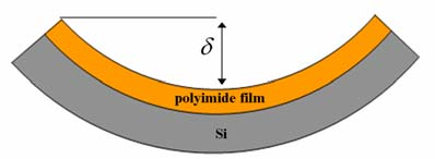
Warpage δ is a measure of the deformation resulting from CTE (Coefficient of Thermal Expansion) mismatch between different layers of a multiple layered structure as seen in Fig. 1. The CTE mismatch stress remains in the wafer during the fabrication, thus causing chip warpage when chips are wafer back-grinding process. To predict the warpage and residual stress, several analytical methods have been proposed . However, most of them are inappropriate for analyzing thin silicon chips in that the substrate is much thicker than polyimide film in these methods: the thickness ratio of polyimide film versus substrate should be less than 1/20 although more enhanced methods have been proposed to cover the higher thickness ratios approximately . In the present study, we employ finite element method (commercial software ABAQUS ) to predict the deformation behavior of thin silicon semiconductor chips.
In addition, there are a few unknown parameters that should be clarified such as material properties of the pattern layer, and stress-free temperatures of materials. The integrated circuit pattern structure on silicon wafer is fabricated through many unit processes such as diffusion, oxidation, metallization, etching and passivation on a silicon wafer, thus naturally consisting of complex and tiny materials. It would be impossible to model the pattern structure considering every tiny and complex component in detail. Therefore, we extract its equivalent material properties by fitting the test results to the CBA (Composite Beam Analysis) together with homogeneity assumption.

Fig1
The pattern layer, which is made of various materials such as silicon nitride (SiN), aluminum (Al), and oxides, consists of several tiny and complex structures including metal lines, metal pads, vias, interlayer dielectric (ILD), shallow trench isolation, barrier metals and inorganic passivation layers. This kind of multiscale structure would not be tractable to a strict computational modeling as it is, i.e., it is too complex to model the entire structure in detail. Accordingly, we assume that this layer is comprised of a single homogeneous material and find the equivalent material properties. The equivalent material properties of the pattern layer are then calculated by fitting measured warpage results to CBA analysis as follows.
上一篇: 紫外激光去除硅晶片中的小金属颗粒
下一篇: 高质量等离子体增强化学气相沉积氮化硅薄膜