The interest in Infrared and Ultraviolet detectors has increased immensely due to the emergence of important applications over a wide range of activities. Detectors based on free carrier absorption known as Hetero-junction Interfacial Workfunction Internal Photoemission (HEIWIP) detectors and variations of these heterojunction structures to be used as intervalence band detectors for a wide wavelength region are presented. Although this internal photoemission concept is valid for all semiconductor materials systems, using a well studied III-V system of GaAs/AlxGa1−xAs to cover a wide wavelength range from UV to far-infrared (THz) is an important development in detector technology. Using the intervalence band (heavy hole, light hole and split offff) transitions for high operating temperature detection of mid Infrared radiation is also discussed. A promising new way to extend the detection wavelength threshold beyond the standard threshold connected with the energy gap in a GaAs/AlxGa1−xAs system is also presented. Superlattice detector technology, which is another promising detector architecture, can be optimized using both Type I and Type II heterostructures. Here the focus will be on Type II Strained Layer (T2SL) Superlattice detectors. T2SL Superlattices based on InAs/(In,GA)Sb have made signifificant improvements demonstrating focal plane arrays operating around 80K and with multiple band detection capability. A novel spectroscopic method to evaluate the band offffsets of both heterojunction and superlattice detectors is also discussed.
Quantum Dot Infrared Photodetectors (QDIP) and Dot In the Well (DWELL) detector structures are also reported in detail in the literature Although QWIP, QDIP and DWELL structures consists of heterojunctions and an interface, the transitions are between two states originating from the quantization effffects inside the well material but not due to free carrier absorption. Hence the superlattice discussion here will be mostly limited to Type II superlattice detectors. InAs and InGaSb like lattice mismatched materials in a periodic pattern can form superlattices generally known as Type II Strained Layer (T2SL) superlattices. Advances in growth techniques etc., and prediction of very high performances has increased the interest in T2SL infrared detectors.
In this chapter, the focus is on photon detection in heterojunction and superlattice devices, although the homojunction detectors are also reported elsewhere . This heterojunction internal photoemission interfacial workfunction (HEI-WIP) detector idea discussed here can be applied to any semiconductor material where an interface associated energy gap can be formed. Varying the interfacial work function will lead to difffferent energy photons to be detected giving rise to difffferent threshold wavelength detectors. This threshold wavelength (λt) is given by λt = 1.24/Δ where Δ is the energy gap. This idea which is valid for both n and p-type structures will be extended to show how multiband detection is achieved in a single detector. In addition controlling the operating temperature and the responsivity by adjusting the interfacial work function will also be discussed in connection with (the p-type) spin-orbit split-offff detectors.
Schottky barrier IR detector proposed by Shepherd et al.,was the fifirst detector type reported as using Internal photoemission (IP). Since then, several difffferent types of internal photoemission detectors have been demonstrated. Among the initial detector developments, the most important types were metal-semiconductor Schottky barrier IR detectors, such as PtSi/Si detectors operating in 3–5 μm range; GexSi1−x/Si detectors developed for 8–14 μm or even longer wavelengths. The absorber/photoemitter “electrode” is a metal or a metal silicide in the Schottky barrier and silicide detectors respectively. A similar detector concept was proposed and demonstrated by Liu et al., using Si MBE multilayer structures in the long-wave infrared (LWIR) range. However, the basic operating mechanism is the same, and following the terminology of Lin and Maserjian, all of these detectors including the free carrier based detectors can be described as Heterojunction or Homojunction Internal Photoemission (HIP) detectors.
The diffiffifficulties of controlling the barrier height and extending the threshold to high wavelengths in homojunction detectors has led to the development of the HEIWIP detectors where the Al fraction in one or both of the layers can control the workfunction. Although the n-type emitters also can provide HEIWIP detectors [see Fig. 1], most of the work on HEIWIP is reported with p-type emitter structures. The band diagram for both n-type and p-type emitter HEIWIP detectors are shown in Fig. 1. The additional degeneracy in the p-type (Heavy hole, Light hole and Splitoffff) has shown to be useful in obtaining an extra control in addition to the Al fraction which will be discussed later.

Fig1
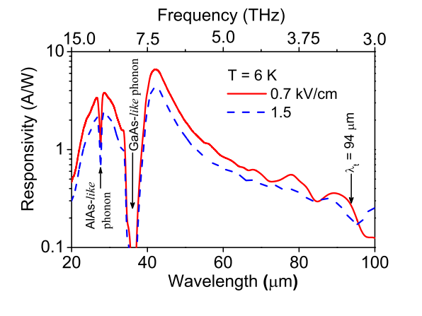
p- type HEIWIP detectors can be categorized into two categories. The fifirst type [Fig. 3(a)] is the standard HEIWIP detector, which uses doped GaAs emitters and undoped AlxGa1−xAs barriers. Here the contributions from the doping and Al fraction to the workfunction are both in the same direction, i.e. decreasing the Al fraction can increase the threshold wavelength from a minimum of ∼ 2.3 μm for an AlAs emitter up to a longer limit of ∼ 110 μm for an Al fraction of 0.005. This is due to the Al fraction at which the Al starts to act as an isoelectronic dopant and does not produce a consistent change in the valence band. Also, x = 0.005 is a practical limit for accurate growth. While an Al fraction of zero is possible, that would correspond to the HIWIP case which had the threshold frequency limitation.
The second type of design uses doped AlxGa1−xAs as the emitter, and undoped GaAs as the barrier as shown in Fig. 3(b). In this approach the band offffset from the Al fraction is used to reduce the band offffset from the doping in the emitter. In this approach, the Al fraction must be kept small (x < 0.17) such that the band offffset does not exceed the doping offffset. In theory, this approach will allow the workfunction to be reduced down to zero.