We achieved room temperature continuous wave operation of a surface emitting two-dimensional photonic crystal diode laser by current injection. This is the first time ever that room temperature continuous wave operation of a photonic crystal diode laser has been realized. This laser features single mode oscillation over a large area, which is impossible for conventional lasers. In this work, we optimized the epitaxial layer composition for better carrier confinement and clarified the relationship between the diameter of the air holes in the photonic crystal and the threshold current of the laser in order to estimate the optimized threshold current.
Photonic crystals , which have a periodic refractive index change, possess great potential for realizing new optical devices. The photonic band-gap is a well-known property of photonic crystals that allows them to block light waves selectively. Many types of two dimensional (2D) photonic crystal lasers, such as defect-mode lasers using the photonic bandgap and artificially-introduced defects or multi-directional distributed feedback (DFB) lasers have been demonstrated. In particular, surface-emitting 2D photonic crystal lasers (Fig. 1) are operated by current injection and have the capability for single mode oscillation over a broad area due to the 2D DFB effect. Broad-area lasers have several advantages, not only in terms of high output power and heat sinking, but they also exhibit a narrow divergence angle.
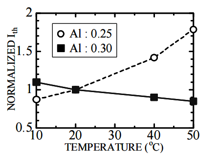
The basic characteristics of the device as a semiconductor diode laser have also been improved. A remarkable reduction in the laser threshold current was successfully realized by reducing the distance between the active layer and the photonic crystal layer to make the 2D photonic crystal effect stronger. The threshold current in this case is 1/25 of the value that we measured in our previous work . Consequently, continuous wave (CW) operation by current injection was achieved. However, the operating temperature was below -20ºC, due to carrier overflow from the active layer. In this work, to produce an increase in the operating temperature of the laser, we confined carriers into the active layer by using a higher band gap AlGaAs layer (aluminum composition: 0.30), which was introduced between the InGaAs/GaAs active layer and the photonic crystal layer. Consequently, the temperature characteristics of the laser are improved and the realization of CW operation at temperatures up to room temperature (RT) can be expected. In addition, it is known that the size of the air holes in the photonic crystal affects the characteristics of photonic crystal devices, though their effect on a laser of this type has not clarified so far. Therefore, in this work, the relationship between the relative volume occupied by the photonic crystal air holes, (known as the air-filling factor) and the threshold current of the laser is revealed, along with improvements in the processing technique.
Wafers of type-B consisted of a GaAs SCH layer, a p-type Al0.4Ga0.6As cladding layer, a GaAs contact layer and an AlGaAs etch stop layer on a p-type GaAs substrate. Air rods (an essential element of the 2D photonic crystal) were formed on wafer A by electron beam lithography and plasma etching. To obtain the as-designed diameter of the photonic crystal, we changed our previous method of drawing hole patterns on resist by electron beam lithography from painting out circular patterns one by one to plotting one dot per each circle. Furthermore, we used inductively-coupled plasma etching for the plasma etching process because we could more easily obtain vertical and uniform photonic crystal air holes and lower sidewall roughness with this technique compared with the reactive ion etching process. The arrangement of the air rods was a square lattice with a depth of about 100 nm. The depth and the distribution of the photonic crystal were determined in order to obtain a coupling coefficient κ of over 1000 cm-1 with sufficient optical confinement in the active layer. The lattice constant was 286.25 nm, which is equal to the lasing wavelength in the material. After the formation of the photonic crystal, one each of wafers A and B were stacked and fused at high temperature, as shown in Fig. 1. The p-type GaAs substrate and the AlGaAs etch stop layer were removed by a mechanical lapping process and chemical etching. After that, an insulating layer of silicon nitride and a square-shaped Ti/Au electrode whose side length was 50 µm, were formed on the surface of the exposed p-type GaAs contact layer.

Fig1
In summary, we have succeeded for the first time in operating a surface-emitting 2D photonic crystal diode laser in CW mode at RT by current injection. We used an Al0.3Ga0.7As subcladding layer between the active layer and the photonic crystal layer to block carriers into the active layer. By using the sub-cladding layer, carriers are confined in the active layer and RTCW operation is successfully realized in this work. We also investigated the relationship between the airfilling factor and the threshold current of the device experimentally, and estimated the threshold current when the air-filling factor is optimized.
The authors would like to thank Dr. Masayuki Fujita, Mr. Shinpei Ogawa, Dr. Eiji Miyai, Mr. Kyosuke Sakai, Mr. Takui Sakaguchi and Mr. Mitsuru Yokoyama for helpful discussions and assistance. This work was partly supported by Core Research for Evolutional Science and Technology - Japan Science and Technology Agency (CREST-JST), 21st Century COE Program - Kyoto University, Kyoto Nanotechnology Cluster (Kyo-nano).
上一篇: 红外探测器的历史
下一篇: 用激光光刻技术连接预特征的单光子发射器