Future quantum optical chips will likely be hybrid in nature and include many single-photon emitters, waveguides, filters, as well as single-photon detectors. Here, we introduce a scalable optical localization-selection-lithography procedure for wiring up a large number of single-photon emitters via polymeric photonic wire bonds in three dimensions. First, we localize and characterize nitrogen vacancies in nanodiamonds inside a solid photoresist exhibiting low background fluorescence. Next, without intermediate steps and using the same optical instrument, we perform aligned threedimensional laser lithography. As a proof of concept, we design, fabricate, and characterize threedimensional functional waveguide elements on an optical chip. Each element consists of one singlephoton emitter centered in a crossed-arc waveguide configuration, allowing for integrated optical excitation and efficient background suppression at the same time.
To bring practical optical quantum information processing to life, single-photon sources3–6, waveguides and splitters, filters, as well as single-photon detectors9,10 need to be integrated into functional quantum-optical chips. The fabrication of such chips, which will likely be hybrid in nature, is a demanding task. In free-space optics, using mirrors on an optical table, it is straightforward to couple a given pre-selected single-photon emitter into an optical setup. Doing likewise on an optical chip is a formidable task. Pioneering experiments have localized and characterized single-photon emitters based on self-organized semiconductor quantum dots by optical microscopy and spectroscopy. By using alignment markers, the subsequent electron-beam lithography could be aligned with respect to these emitters. More recently, even in-situ lithography of basic light collecting structures around quantum dots was reported. Other experiments have moved nanodiamonds containing nitrogen-vacancy (NV) centers as single-photon emitters to desired locations on surfaces by means of an atomic-force microscope15 or with tungsten micromanipulators.
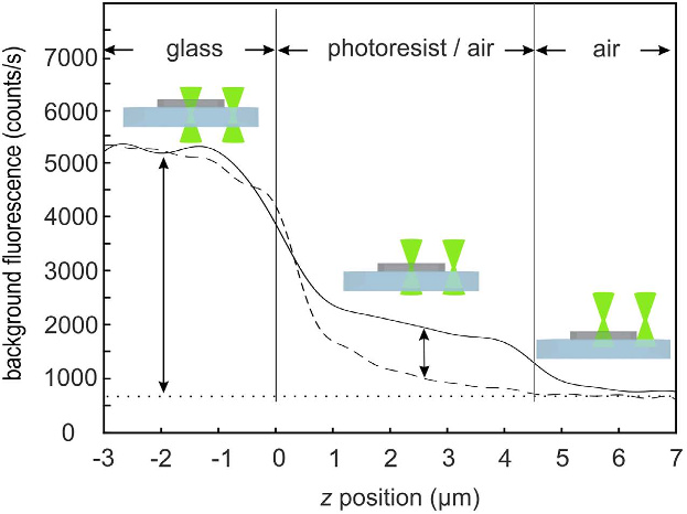
Two requirements regarding the photoresist are crucial. Fulfilling both of them simultaneously is highly nontrivial. First, the photoresist must be solid as the nanodiamonds could move in a liquid. However, most high-end photoresists for 3D optical laser lithography are liquid20. Second, the photoresist must exhibit low background fluorescence – prior to exposure as well as after polymerization.
We note in passing that this pre-selection process is not restricted to NV centers in nanodiamonds. For example, silicon-vacancy centers in nanodiamonds with narrower spectral emission are emerging. Furthermore, one could also select with respect to charge state, quantum efficiency, and dipole orientation. In principle, any other type of emitter is possible.
In conclusion, we have introduced a localization-selection-lithography approach and a low-background-fluorescence photoresist to fabricate three-dimensional quantum optical functional elements. The method is highly scalable, possesses high yield, and can be fully automated. A next step could be to wire-up several quantum emitters via one waveguide to realize an efficient source of photon Fock states with N>1. In this respect, silicon-vacancy centers in nanodiamonds may be more appropriate than NV centers. The waveguides could also be aligned with respect to the a priori randomly oriented emitter dipoles. Another attractive possibility is to introduce a second fabrication step, for example partial metallization in order to fabricate pre-aligned three-dimensional plasmonic antennas30 to enhance single-photon emission or microwave antennas to perform optically detected magnetic resonance (ODMR). Finally, our platform is fully compatible with microfluidics. Therefore, besides quantum optics, our approach could be useful for advanced nano-sensors, in which photon generation, collection, as well as optically-enhanced ODMR would all be integrated in one multi-functional element.

Fig1
Measurement setup: We used the same components as in the setup for the fabrication (see above). However, we tilted a mirror in the optical path imaging the sample plane onto the intermediate image plane. In this fashion, we effectively moved the position of the pinhole relative to the intermediate image plane, such that we could pump into any one of the four waveguide ports and collect the emission from any other one of the four ports. For efficient collection via a microscope with an optical axis normal to the substrate plane, the waveguide axes at the substrate needed to be normal to glass substrate plane.
It was difficult to estimate the in-coupling efficiency of the pump beam into the waveguide. Thus, to obtain the order of magnitude for the collection efficiency of single-photon emission into the double-arc waveguide structure, we compared the measured saturation count rates. These were defined as half of the maximum possible count rates for very large pump power. The saturation count rates were obtained by fitting to saturation measurements like shown in Fig. 4d,f. From Fig. 4d, we obtained a saturation count rate of about 19,000 counts/s for one port, hence roughly 76,000 counts/s for all four ports. For the conditions as in Fig. 1, we obtained typical saturation count rates of 125,000 counts/s for roughly one half of the total solid angle (assuming the emission pattern of a dipole oscillating parallel to the substrate plane), thus 250,000 counts/s roughly estimated for the total solid angle. The collection efficiency was thus about 30%.
下一篇: 集成 TOSA 和高速EML 芯片