Spin-coating photoresist film on ZnO nanowire (NW) was introduced into the fabrication procedure to improve photoresponse and recovery speed of a ZnO NW ultraviolet photoelectric detector. A ZnO NW was first assembled on prefabricated electrodes by dielectrophoresis. Then, photoresist was spin-coated on the nanowire. Finally, a metal layer was electrodeposited on the nanowireelectrode contacts. The response properties and I-V characteristics of ZnO NW photodetector were investigated by measuring the electrical current under different conditions. Measurement results demonstrated that the detector has an enhanced photoresponse and recovery speed after coating the nanowire with photoresist. The photoresponse and recovery characteristics of detectors with and without spin-coating were compared to demonstrate the effects of photoresist and the enhancement of response and recovery speed of the photodetector is ascribed to the reduced surface absorbed oxygen molecules and binding effect on the residual oxygen molecules after photoresist spin-coating. The results demonstrated that surface coating may be an effective and simple way to improve the response speed of the photoelectric device.
ZnO is a semiconductor material with a direct energy band gap of 3.37 eV and a large excitation binding energy of 60 meV at room temperature. Different fields have studied the potential applications of ZnO, such as transistors, photodetectors, piezoelectric devices, solar cells, and sensors. Recently, ZnO semiconductor nanowires, nanobelts, and nanoparticles with characteristic of high surface-to-volume ratios have emerged as remarkable nanomaterials in various fields. For example, Soci demonstrated that the optical internal gain of ZnO nanowire (NW) ultraviolet (UV) photodetectors could reach as high as ~108 , and this gain shows their potential application in gain-bandwidth products. However, two fundamental limitations remain to be overcome.
Surface functionalization has been proved to be an effective way to modify surface physical properties of ZnO NWs. Indeed, it can be used to enhance the electrical and optoelectronic performance of ZnO NW devices. However, the functionalization processes for the fabrication of ZnO solid vapor process under controlled conditions . ZnO NWs were suspended in an ethanol solution by sonication. Figure 2 briefly illustrates the fabrication procedures of the basic photodetector. The parallel electrode patterns were defined by a standard photolithography procedure.

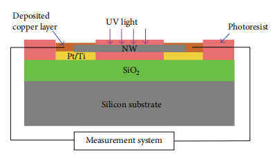
The structural diagram of a ZnO NW-based photoelectric photodetector is illustrated in Figure 1. Pt electrodes were fabricated on a silicon substrate and were isolated by an 800 nm SiO2 layer. ZnO NW was assembled on the Pt electrodes to form the channel of carriers, which could detect UV photons. The photoresist coating is isolated O2 from the ambient atmosphere. Thus, the absorption and desorption processes of O2 were prevented and thus the response and recovery speed of the photodetector were enhanced. Two electrodes were electrodeposited by the metal layer to form good metal-semiconductor contact with the help of the photoresist pattern. At the same time, the deposited copper used in this work had a lower work function than the Pt electrodes, and the deposited copper layer could enlarge the contact area of the metal-semiconductor contacts, thus forming ohmic-type metal-semiconductor contacts.
I-V Characteristics of the Nanowire Photodetector. Figure 4 compares the typical I-V characteristics of the nanowire photodetector without photoresist coating before (red curve) and after (black curve) electrodeposition. I-V characteristics were measured at room temperature by the picoammeter under dark conditions. The black curve shows a noticeable decrease in resistance compared with the red curve; this decrease demonstrates that a good ohmic-type device was fabricated after electrodeposition. This decrease may be due to the fact that the work function of copper (4.51 eV) is closer to the electron affinity of ZnO (4.1 eV) than the work function of platinum (5.64 eV). At the same time, the deposited copper covering on the Pt electrodes and nanowire can enlarge the contact area of metal-semiconductor contacts.
上一篇: 锑化镓物理与技术:一种新兴的光电材料
下一篇: 在负性光刻胶上制造悬浮微结构的方法