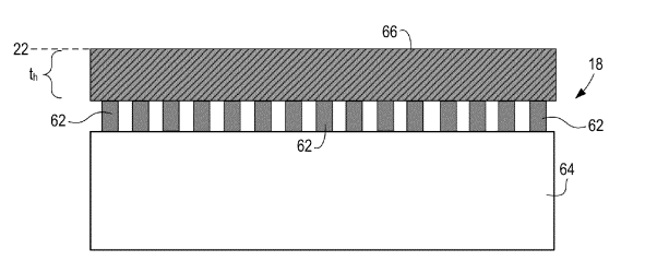
Porous nano-imprint lithography templates may include pores, channels, or porous layers arranged to allow evacua tion of gas trapped between a nano-imprint lithography tem plate and substrate. The pores or channels may be formed by etch or other processes. Gaskets may be formed on an nano imprint lithography template to restrict flow of polymerizable material during nano-imprint lithography processes.
Nano-fabrication includes the fabrication of very small structures that have features on the order of 100 nanometers or Smaller. One application in which nano-fabrication has had a sizeable impact is in the processing of integrated circuits. The semiconductor processing industry continues to strive for larger production yields while increasing the circuits per unit area formed on a substrate; therefore nano-fabrication becomes increasingly important. Nano-fabrication provides greater process control while allowing continued reduction of the minimum feature dimensions of the structures formed. Other areas of development in which nano-fabrication has been employed include biotechnology, optical technology, mechanical systems, and the like.
An imprint lithography technique disclosed in each of the aforementioned U.S. patent publications and patent includes formation of a relief pattern in a polymerizable layer, and transferring a pattern corresponding to the relief pattern into an underlying Substrate. The Substrate may be coupled to a motion stage to obtain a desired positioning to facilitate the patterning process. The patterning process uses a template spaced apart from the Substrate and a formable liquid applied between the template and the substrate. The formable liquid is Solidified to form a rigid layer that has a pattern conforming to a shape of the surface of the template that contacts the form able liquid. After solidification, the template is separated from the rigid layer such that the template and the substrate are spaced apart. The substrate and the solidified layer are then subjected to additional processes to transfer a relief image into the Substrate that corresponds to the pattern in the solidified layer.
In some implementations, the electromagnetic radiation includes laser irradiation with a pulse length of less than about 100 nanoseconds. The covered recesses may define openings with a dimension less than about 10 nm. In certain cases, oxidizing includes heating.

Fig1
In some implementations, the side walls of the recesses may be protected before a volume of the recesses is adjusted. In certain cases, adjusting a Volume of the recesses may include isotropically etching a bottom of the recesses to enlarge a Volume of the recesses.
Gas escape and dissolution rates may limit the rate at which the polymerizable material is able to form a continuous layer on the Substrate (or imprinting stack) or the rate at which the polymerizable material is able to fill template features after the template contacts the polymerizable material, thereby limiting throughput in nano-imprint processes. For example, a substrate or a template may be substantially impermeable to a gas trapped between the Substrate and the template. In some cases, a polymeric layer adhered to the Substrate or the tem plate may become saturated with gas, Such that gas between the imprinting Stack and the template is Substantially unable to enter the Saturated polymeric layer, and remains trapped between the Substrate and the Substrate or imprinting stack. Gas that remains trapped between the substrate or the imprinting stack and the template may cause filling defects in the patterned layer.
In some cases, the Substrate/imprinting Stack or template may include a porous material defining a multiplicity of pores with an average pore size and pore density or relative porosity selected to facilitate diffusion of a gas into the substrate/ imprinting stack or the template, respectively. In certain cases, the Substrate/imprinting stack or template may include one or more layers or regions of a porous material designed to facilitate transport of gases trapped between the Substrate/ imprinting stack and the template in a direction away from the polymerizable material between the substrate/imprinting stack and Substrate and toward the Substrate/imprinting stack or the template, respectively.
上一篇: 化学镀金工艺优化
下一篇: 通过掩模电镀沉积镍薄膜微结构的均匀性控制