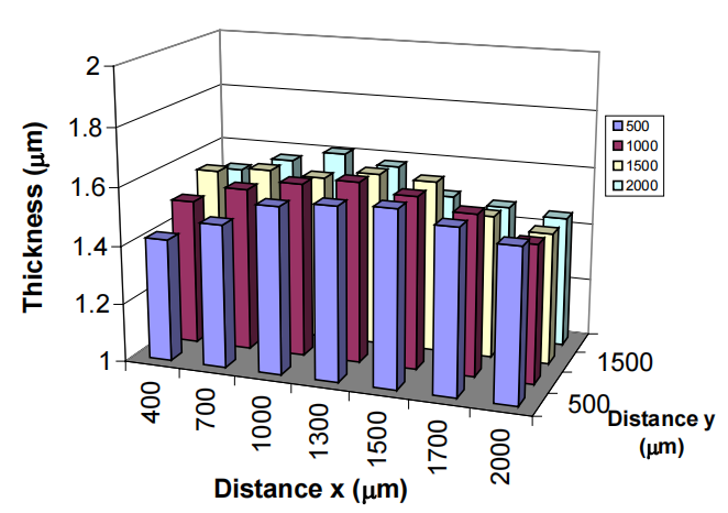
The thickness uniformity within a specimen and the cross-sectional profiles of electroplated individual Ni-microstructures have been investigated as a function of the electroplating conditions. It was found that the uniformity and profiles of microstructures could be controlled by varying the process conditions. A uniform thickness distribution and microstructures with flat profiles could be obtained at optimal plating conditions of 8mA/cm2 and 60°C. Above this optimal plating current density, the microstructure has a rabbit-ears profile and the thickness of a narrow microstructure is thicker than that of wide ones. While below this current density, the microstructure has a cap-like cross-sectional profile, and a narrow structure is thinner than wide ones. Increasing the plating temperature enhances the non-uniformity, whereas other process parameters have insignificant effects on it. The current crowding observed in patterned specimens is responsible for the rabbit-ears profile of individual microstructures, while a combination of the fluidic friction on the sidewall of the photoresist and the electrophoresis of the ions in the solution are believed to be responsible for the abnormal cap-like profile of individual microstructures and the thinning effect on narrow microstructures.
Electrodeposition (or electroplating) has become one of the most important technologies for microelectronics and microelectromechanical systems (MEMS), as it produces high quality metal films in a simple way at a low-cost. Various metal and alloy films such as Ni, In, Cu, Au and NiFe, NiP, CoFe have been formed by electrodeposition.A combination of photolithography technology and electrodeposition (so-called through mask plating4 ) makes it possible to fabricate microstructures suitable for microsensors and microactuators. However one of the problems associated with electrodeposition is the uniformity control of the electroplated films both in thickness and composition. This affects the material properties and resulting performance of micro-components.
The plating solution was commercially purchased from Celtic Chemicals Ltd, and consisted of nickel sulphamate (300 g/l), nickel chloride (10 g/l) and boric acid (40 g/l). The pH value of the as-made plating solution was 3.8, which gradually increased to around 5.0 after plating up to approximately one hundred times. A Ni plate with an area of ~ 4 cm2 was used as the anode. A magnetic pellet was used to stir the solution to keep the concentration uniform and to prevent the formation of hydrogen bubbles on the sample surface. The plating temperature was varied in the range 20 - 80 °C with ± 2 °C accuracy, and the current density was varied in the range 1 - 30 mA/cm2 .

Fig1
The combination of these two models can also explain the effects of other process parameters qualitatively. As long as the ion concentration is sufficient to provide the plating reaction, the effect on the profile of individual microstructures and the thickness distribution is insignificant, as the profile is determined by the thickness of the boundary layers and the degree of the current crowding. Other causes that may be responsible for the abnormal profile include the potential perturbation by the photoresist sidewall and the impurities absorbed.
上一篇: 纳米压印光刻模板
下一篇: LCOS 和 AR或VR