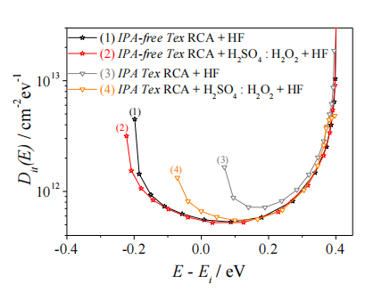
The application of an Isopropanol(IPA)-free potassium hydroxide (KOH) solution was evaluated in order to prepare random pyramids on as-cut crystalline n-type Si wafers to reduce reflection losses of substrates for high-efficiency hetero-junction solar cells. The influence of saw damage removal and texturization processes on the resulting pyramid morphology and the corresponding interplay between optical and electronic properties are revealed. It is shown that both the depth of the saw damage etching (SDE) and the duration of the texturization etching have crucial influence on the resulting pyramid size distribution. Reflection losses can be reduced with decreasing fraction of small pyramids. By intermediate saw damage removal and texture etching times in (IPA)-free KOH solution the densities of electronic interface states were found to be strongly decreased (Dit,min < 5 10-11 cm-2eV-1), in comparison to pyramids prepared in IPA containing solutions. For the purpose of fabricating amorphous/crystalline (a-Si:H/c-Si) heterojunction solar cells the Si substrate surfaces were passivated with an intrinsic layer of amorphous silicon (aSi:H(i)) leading to minority charge carrier lifetimes eff of 2 to 4 ms, depending on the preceding texturization process.
Selection and/or peer-review under responsibility of the scientififi c committee of the SiliconPV 2013 conference absorption probability by light trapping. Since this improvement of the optical properties is associated with the creation of a larger surface area, the density of electronic defect states is expected to increase, compared to flat substrate surfaces . Conventionally, random pyramid textures are achieved by wetchemical etching of the as-cut wafer in alkaline solution containing IPA as additive. Due to its high volatility and environmental impact IPA was replaced by GP Alkatex Zero. While in industrial processes saw damage removal and texture etch are done in a single process step in this study the two steps are separated to reveal the particular influence of both processes on the pyramid morphology. The correlation of saw damage removal and texturization was investigated with the goal to optimize systematically the resulting pyramid morphology with respect to minimal reflection and recombination losses.
Reflection losses were analyzed with a Perkin Elmer Lambda 1050 UV-Vis-NIR spectrometer with integrated sphere. Spectra were taken in the range of 250 nm to 1500 nm. For significant comparison of the samples the normalized reflection Rn was considered. Rn is derived from the ratio of the integrated UV-Vis reflection spectra in the range of 250 nm to 1200 nm and the complete reflection (100 %) in this interval.

Fig1
In the upper row of Fig. 3 SEM images of samples only treated with SDE are shown. The SEM image of the sample with only 5 μm/side SDE (Fig. 3a) clearly shows an increased inhomogeneity compared to a sample with intermediate (10 μm/side) saw damage removal (Fig. 3b). For a higher saw damage removal of 20 μm/side (Fig. 3c) only a marginal improvement of homogeneity is found.
The lower row of Fig. 3 shows SEM images of similarly saw damage etched samples after subsequent texturization etching of 20 min. As shown in the SEM images of Fig. 3 due to the low depth of saw damage removal (5 μm/side) the texturization process does not completely eliminate the inhomogeneities at the surface (1), compared to the samples with higher depth of damage removal (2) and (3). Moreover intermediate saw damage removal results in a surface with bigger pyramids (2). Even at the surface of the sample with deeper SDE a higher fraction of small pyramids was obtained (3).
The inset of Fig. 4 presents the resulting the minority charge carrier lifetimes eff determined by TrPCD measurements on identically prepared samples (set A) after deposition of intrinsic amorphous silicon (a-Si:H(i)) layers and post-deposition hydrogenation. It is shown, that for all samples an appropriate passivation of defects is achieved. Highest carrier lifetime eff is obtained by intermediate saw damage removal (e.g. (2), approx. 4 ms). A lower (1) as well as a further saw damage removal (3) result in lower values of eff of approx. 2.8 and 2.4 ms, respectively. As a reason for the decrease of charge carrier lifetimes after longer SDE we assume the longer overall etching duration and the corresponding appearance of a higher number of smaller pyramids and therefore an increased number of pyramid valleys. Pyramid valleys are known to cause defects at the a-Si:H(i)/c-Si interface. Furthermore many smaller pyramids cause additional defects due to an enlarged roughness at the surface.
上一篇: LCOS 和 AR或VR
下一篇: 不同掺杂剂锗硅单晶的张电阻特性