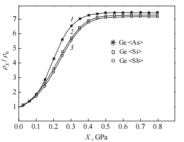
Tensoresistance in single crystals of germanium and silicon with different dopants but under practically equal charge carrier concentrations have been investigated.The features of ρX /ρ0 = f (X) function, which depend on individual physical-chemical properties of dopants, have been discussed in this paper.
Electronic properties of many-valley semiconductors are determined by their band structure as well as availability, energy spectrum and spatial distribution of electrically active impurities and defects in the bulk of crystal. With mass production of semiconductor electronics devices, to meet the modern requirements of reproducibility and stability of their characteristics is possible only when using materials with high homogeneity of parameters. This is particularly important in microelectronics in the manufacture of large- and very large-scale integrated microcircuits and power semiconductor devices. Today, it became clear that further increasing the density of integrated microcircuits, their reliability and efficiency, obviously, can not be realized only by improving technology and restricting microinhomogeneities of physicochemical properties in semiconductor materials. Therefore, the problem of microinhomogeneities research has been and remains urgent to date.
Defects are usually separated by two large groups: 1) one-dimensional, two-dimensional, three-dimensional ones that disturb the crystal structure at considerable distances; 2) point defects that disturb the crystal structure over relatively small distances. The first group includes dislocations, dislocation networks, grain boundaries and twins, different defects of packing, nuclei of a new phase, clusters of point defects. These defects are formed, as a rule, in the process of growing crystals, during plastic deformation, as well as under irradiation by heavy particles of a high energy.
Impurity atoms are the second major type of point defects, which are introduced into the semiconductor crystal during its growth, as well as under diffusion or by ion implantation. These point defects can be placed both in the lattice sites, and in the interstitial positions of the crystal lattice. If the impurity atom in its physical and chemical properties is similar to the atoms of matrix, then it is usually placed in a vacant lattice site. In the case when its properties are very different from those of matrix atoms, it is located between the lattice sites. In many-valley semiconductors, all atoms of the periodic system can serve as impurities. This fact allows obtaining a wide range of electronic properties of crystals.

Fig1
When the concentration of dopant impurity rises, interaction between impurity atoms appears and their energy levels are changed just as the atomic electronic levels split in the band during formation of the crystal. The impurity band appears as a result of this interaction. When the concentration of the impurity atoms with shallow levels is higher than 1018 сm-3, their ionization energy is reduced to almost zero as a result of the expansion of the impurity band and its confluence with the conduction or valence bands. Semiconductor acquires metallic properties; it becomes a semimetal or a degenerate semiconductor.
Dopant impurities affect on the character of charge carriers movement, and the latter are scattered by the ionized and neutral impurity atoms, which significantly affects on the phenomena of electronic transport. Impurity atoms, as a lattice defects, affect on the other physical, chemical, optical, and magnetic properties of semiconductors, as well as actively interact with the radiation defects. These processes lead to the change in the energy spectrum of the impurity states in the forbidden band.
Characteristic features of the physical properties of many-valley semiconductors are determined by the symmetry of crystal lattice and the nature of interatomic interaction. To investigate crystals, uniaxial elastic deformation is often applied, which causes the change not only in interatomic distances but also in symmetry of lattice, and results in the most significant changes in their energy spectrum. This, in turn, determines the corresponding changes in their electronic properties, the study of which provides the valuable information about the investigated object.
上一篇: n 型硅晶片的无IPA纹理化
下一篇: 化学机械抛光的逐次运行控制