The “River Publishers Series in Electronic Materials and Devices” is a series of comprehensive academic and professional books which focus on the theory and applications of advanced electronic materials and devices. The series focuses on topics ranging from the theory, modeling, devices, performance and reliability of electron and ion integrated circuit devices and interconnects, insulators, metals, organic materials, micro-plasmas, semiconductors, quantum-effect structures, vacuum devices, and emerging materials. Applications of devices in biomedical electronics, computation, communications, displays, MEMS, imaging, micro-actuators, nanoelectronics, optoelectronics, photovoltaics, power ICs and micro-sensors are also covered.
Books published in the series include research monographs, edited volumes, handbooks and textbooks. The books provide professionals, researchers, educators, and advanced students in the fifield with an invaluable insight into the latest research and developments.
This book is distributed under the terms of the Creative Commons Attribution-NonCommercial 4.0 International License, CC-BY-NC 4.0) (http://creativecommons.org/ licenses/by/4.0/), which permits use, duplication, adaptation, distribution and reproduction in any medium or format, as long as you give appropriate credit to the original author(s) and the source, a link is provided to the Creative Commons license and any changes made are indicated. The images or other third party material in this book are included in the work’s Creative Commons license, unless indicated otherwise in the credit line; if such material is not included in the work’s Creative Commons license and the respective action is not permitted by statutory regulation, users will need to obtain permission from the license holder to duplicate, adapt, or reproduce the material.

Fig1
The basic structure of the aforementioned DPSA-SEG process flflow was already employed for the fifirst demonstrations [Sat92, Mei95, Pru95]. Essentially, it has been maintained to date. In Figure 1.7, a TEM cross section of Infifineon’s latest SiGe HBT transistor generation is shown.
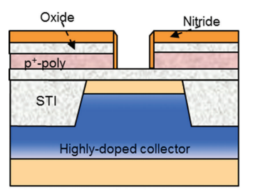
The collector construction used by Hitachi [Has14], Infifineon [Boe15], and STMicroelectronics [Che14] includes all elements which are typical for a high-speed Si bipolar transistor: an epitaxially buried, highly doped subcollector isolated laterally by deep trenches and a low-ohmic connection to the collector contact realized by a so-called collector sinker. In order to save fabrication efforts and to reduce complexity of the BiCMOS process, NXP (former FreeScale) developed a Sub-Isolation Buried Layer (SIBL) collector structure using only shallow trench isolation (STI) [Joh07]. A common feature of all these technologies is the shallow-trench isolation (STI) between the internal transistor region and the collector contact which enables simultaneously a low capacitive base link.
If the geometry of a conventional DPSA-SEG SiGe HBT (see Figure 1.6(d)) is shrunk according to scaling scenarios for next technology nodes, as it was carried out in TCAD studies [Sch11b, Sch17], there is no serious indication for an imminent end of performance progress compared to other technology approaches. In practice, however, we are confronted with the fact that the attempts to increase f MAX did not go beyond values of 400 GHz while alternative concepts indeed surpassed this level. Unfortunately, the main reason for this defificiency is closely connected with the key advantage of the conventional DPSA-SEG process, namely the straightforward manufacturing of the link between the intrinsic transistor region and the base poly-Si layer.
In the fifirst publication on this technology concept [Fox11] f T/f MAX/CML gate delay values of 300 GHz/480 GHz/1.9 ps were presented. However, a detailed comparison of the EBL HBT performance against standard DPSASEG results was not in the focus of this fifirst demonstration. This assessment has been addressed in the DOTSEVEN project. The EBL HBT was compared directly with the conventional DPSA-SEG approach based on identical collector designs, transistor layouts, and measurement conditions. For this purpose, the EBL HBT module was implemented in Infifineon’s 0.13 µm BiCMOS environment which includes the standard collector concept of an epitaxially buried sub-collector and deep-trench (DT) isolation combined with a mm-wave Cu back-end-of-line (BEOL). In contrast, the original EBL process comprised IHP’s DT-free collector approach [Hei02] using STI-isolated, highly doped collector regions as well as an Al-based BEOL.
上一篇: 化学机械抛光的逐次运行控制
下一篇: 硅上的低温锗薄膜