We discuss thermal evaporation of Germanium thin films as a suitable route to realizing near-infrared detectors integrated on a Silicon platform. We study the structural properties of samples grown at various substrate temperatures by X-ray diffraction and transmission electron microscopy, showing that Ge thin films are amorphous when deposited below 225°C, mono-crystalline between 225 and 400°C, poly-crystalline above 450°C. We further investigate their optical and electrical properties using differential optical absorption spectroscopy, Hall and photocurrent measurements. Finally, with the evaporated Ge thin films we demonstrate near-infrared photodiodes with low dark current density and good responsivity at 1.55 µm.
In recent years, Silicon photonics has gained a leading role in applied physics and optical engineering. To date, several photonic and optoelectronic components have been successfully integrated on a Silicon platform exploiting several processes of the standard microelectronics industry. However, the challenge of integration is still open because of the technological problems that prevent a viable monolithic integration of near-infrared (NIR) sensing devices with Si electronics. In fact, while Silicon is an indirect bandgap semiconductor transparent at NIR communication wavelengths, NIR laser sources and detectors require smaller bandgap materials, mostly III-V compounds which are essentially incompatible for integration with standard Si technologies. In this context, Germanium-onSilicon has been recognized as the best alternative towards the monolithic integration of NIR detectors on Silicon platforms, with high performance Ge-on-Si detectors recently demonstrated. Nonetheless, the monolithic integration of Ge photodiodes with standard Si electronics is still hindered by compatibility issues, i. e. thermal budget and crosscontamination stemming from Ge deposition. Although several Ge-on-Si deposition techniques have been successfully implemented, most of them require high temperatures which can hardly coexist with standard CMOS technology. Recently, we have proposed physical vapor deposition of Ge on Si by thermal evaporation (TE) as a viable lowtemperature growth process and demonstrated optoelectronics devices by integrating Ge-on-Si photodetectors with either CMOS circuitry or Silicon photonics elements. However, a detailed analysis and understanding of TE Germanium thin films on Si is still lacking.
In this Paper we report a comprehensive characterization of structural, optical and electrical properties of Ge thin films thermally evaporated on Si. We show hereby that, by simply controlling the substrate temperature, it is possible to grow Ge thin films of different crystalline qualities, obtaining mono-crystalline epitaxial Ge at temperatures in the range 250- 400°C. Finally, we discuss this approach towards fabricating efficient NIR detectors for Si optoelectronics.
Ge thin films were grown on Si by thermal evaporation in a vacuum chamber with a background pressure of 10−8 Torr and about 10−7 Torr during deposition. The material source was high purity (99,999%) small grains of Ge in a tungsten crucible; the substrates were either (100) Silicon or Silicon-on-Insulator (SOI) wafers, carefully cleaned in a standard RCA solution. Prior to Ge deposition, the native silicon-oxide was removed from the substrate surface by chemical etching with buffered hydrofluoric acid (buffered oxide etching - BOE); this pre-TE treatment was a crucial step in obtaining crystalline films. Besides removing the native oxide, BOE also played the important role of passivating the Si surface by terminating the dangling bonds with hydrogen-ions; an H-passivated surface is chemically robust and resistant to oxidization, permitting to handle the specimens in air before placing them in a vacuum. During deposition the evaporation rate was kept constant at about 2 Å/s, whereas the substrate temperatures could be adjusted from 200 to 500°C.

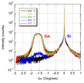
Fig1
In order to further investigate the structural properties of both mono- and poly-crystalline TE samples we resorted to high-resolution (HR) TEM. The results are displayed in Fig. 4 with the insets showing the Fourier transforms (FT) of the HR images. While Ge layers at 300°C are mono-crystalline (epitaxial), those at 500°C have diffractograms typical of a polycrystalline structure, possibly columnar with individual columns differently oriented. We evaluated the intensity distribution of the FT spatial frequencies in order to determine which region corresponded to a particular frequency; the results in Fig. 5 clearly indicate that the Ge layer is structured in columns.
We measured the near-infrared (1200-1650 nm) absorption spectra of amorphous and epitaxial Ge films on Si using differential optical absorption spectroscopy and compared them with reference bulk Ge, as Fig. 6 shows. The amorphous Ge films exhibit an optical absorption slowly decreasing with wavelength without any specific features in the proximity of the Ge bandgap. The spectra of epitaxial Ge films are comparable with those from bulk Ge up to the cutoff wavelength, namely 1550 nm. At longer wavelengths bulk Ge shows the sharp transition corresponding to its direct bandgap (about 0.8eV), whereas the TE thin film spectra have a smooth variation, attributed to the high dislocation density. In particular, dislocations introduce electronic levels in the forbidden bandgap available for energy transitions ; when the photon energy is comparable with the gap between the valence band and the dislocation levels, some photons are still absorbed. In addition, the measurement reliability worsens beyond the gap as the increased transparency eases a number of multiple reflections in the film thickness. The results demonstrate that both amorphous and crystalline evaporated Ge films have significant NIR absorption and can be employed for light detection. However, as we demonstrated earlier, the transport properties of the TE amorphous Ge are not well suited for realizing optoelectronic devices.
上一篇: 用于毫米波系统的硅锗异质结双极晶体管
下一篇: 结晶锗和硅的电子光谱