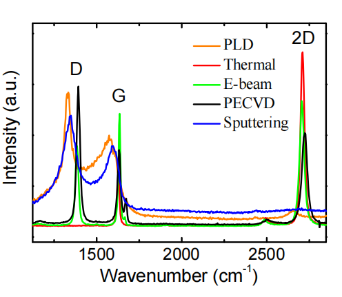
Deposition of various materials onto graphene without causing any disorder is highly desirable for graphene applications. Especially, sputtering is a versatile technique to deposit various metals and insulators for spintronics, and indium tin oxide to make transparent devices. However, the sputtering process causes damage to graphene because of high energy sputtered atoms. By flipping the substrate and using a high Ar pressure, we demonstrate that the level of damage to graphene can be reduced or eliminated in dc, rf, and reactive sputtering processes.
Graphene has attracted enormous scientific and engineering interest due to its superior electronic, optical, thermal, mechanical properties1-9. The important properties of graphene include a high intrinsic charge carrier mobility and a tunability of its properties by applying a gate bias voltage. In order to make top-gate graphene field effect transistors (G-FET), a high-k dielectric gate material needs to be deposited onto graphene without damage, because the mobility of graphene is outstanding when graphene is pristine.10,11 The other interesting application is spintronics, in which an extremely long spin diffusion length or spin lifetime is preferred possibly due to the weak spin-orbit coupling strength.12,13 In order to achieve efficient spin injection, high quality ferromagnetic contacts and tunnel barriers are essential without degrading the intrinsic properties of graphene during the deposition. All of these emphasize the great importance of a nondestructive deposition technique in constructing graphene devices for both fundamental studies and practical applications.
Although graphene is the strongest material ever known4,5, but since graphene is only one monolayer of carbon atoms packed into a two-dimensional honeycomb lattice, the C-C bonds are easy to be broken during the deposition. Therefore, only thermal evaporation is known to be a non-destructive method of deposition onto graphene, which greatly limits the choice of materials in graphene devices. Sputtering is a widely used technique in industries for hard disk drives and for indium tin oxide coating as well as in the spintronics community. However, high energy atom bombardment induces a large amount of disorder into graphene, which greatly degrades the graphene’s property. There have been a few studies based on sputtering onto graphene and all of them exhibited significant disorder.
In this letter, we propose a defect-free sputter deposition technique onto graphene by flipping the sample at high Ar pressure during the deposition in order to reduce the energy of incident sputtering atoms. We investigate different sputtering techniques such as dc, rf, and reactive sputtering, and study the level of damage of graphene by Raman spectroscopy. By flipping the samples and sputtering at high Ar pressure (20 mTorr), we successfully reduce the degree of disorder to a negligible level.

Fig1
In conclusion, we report a method for sputtering onto graphene without disorder by flipping the sample holder in a high Ar pressure. Negligible disorder is observed from the Raman spectra of graphene after the deposition of CoFe and Al by dc sputtering, and the AFM images show a small roughness of the films on graphene. MgO deposited by rf sputtering induces large disorder onto graphene due to its enhanced bombardment effect. However, reactive sputtering of MgO onto graphene leads to a small disorder compared to rf sputtering. The availability of sputtering for the deposition of various materials in the graphene system will pave a way of rigorous material engineering for various graphene applications.
We check the uniformity of deposited materials onto graphene by the proposed sputtering method. Figure 4 shows the atomic force microscopy (AFM) images of 4 nm CoFe and 2 nm Al on graphene which were deposited by the flipping method with 20 mTorr Ar pressure. The mean roughness of CoFe on graphene is 0.432 nm, while that of Al is 0.284 nm. The films show a good uniformity promising for practical applications.
Reactive sputtering is an alternative method to deposit high quality tunnel barriers in a reactive gas mixture with Ar.22 We have deposited 1 nm MgO onto graphene by dc reactive sputtering with the flipping method and the Raman spectra is shown in Fig. 3(d). A small D peak is observed, which comes from the oxygen plasma due to the oxygen gas mixture. By utilizing the proposed flipping method in high Ar pressure, a better quality of graphene is obtained after the oxide deposition as compared to the previous reports14,16,23, which will enable to use various oxide materials in graphene devices by sputtering. Especially, highly spin filtering MgO tunnel barriers are of great importance for spintronic applications. By replacing the O2 gas with the N2 or other reactive gases, various nitrides and other materials can be explored with graphene using reactive sputtering.
上一篇: 硅、锗和硅锗光电池在热光伏中的应用
下一篇: 超出电信波长范围的硅基光子的集成