In this paper we discuss silicon-based photonic integrated circuit technology for applications beyond the telecommunication wavelength range. Silicon-on-insulator and germaniumon-silicon passive waveguide circuits are described, as well as the integration of III–V semiconductors, IV–VI colloidal nanoparticles and GeSn alloys on these circuits for increasing the functionality. The strong nonlinearity of silicon combined with the low nonlinear absorption in the mid-infrared is exploited to generate picosecond pulse based supercontinuum sources, optical parametric oscillators and wavelength translators connecting the telecommunication wavelength range and the mid-infrared.
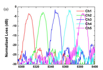
Silicon-on-insulator has become a standard material platform for the integration of photonic devices in the telecommunication wavelength window. Well-developed processes are available including high quality waveguide definition germanium epitaxy etc. Therefore we have explored the use of this material platform for operation at longer wavelengths, using the standard silicon photonics technology that is used today in multi-project wafer approaches. These waveguide structures consist of a 220 or 400-nm thick silicon waveguide layer on a 2-μm thick buried oxide layer on a silicon substrate. Using this technology very low waveguide losses (∼0.5 dB/cm) in the 2–2.5-μm wavelength range have been obtained. Similarly, on the 400 nm silicon waveguide platform 3-dB/cm waveguide losses at a wavelength of 3.8 μm were obtained. Besides low-loss waveguides, functional components for spectroscopic sensing systems were also demonstrated, including planar concave grating spectrometers and arrayed waveguide gratings in the 2–2.5 μm and 3.8-μm wavelength range. The transmission spectrum of a silicon-on-insulator wavemeter (a wavelength demultiplexer circuit where the output channels intentionally overlap in order to accurately measure the wavelength of a laser line injected into the spectrometer through centroid detection) based on an arrayed waveguide grating is shown in Fig. 1(a). This device is implemented on the 220-nm silicon waveguide platform and measures 525 μm by 775 μm. Fig. 1(b) shows the transmission spectrum of a planar concave grating spectrometer operating at 3.8 μm implemented on the 400-nm silicon waveguide platform.
While silicon-on-insulator waveguide circuits are ideal for long-wavelength photonic integrated circuits operating in the 2 to 4-μm wavelength range, the SiO2 buried oxide layer starts absorbing heavily beyond that wavelength. Also the leakage to the silicon substrate through the standard 2-μm thick SiO2 layer becomes an issue. Therefore alternative silicon-based waveguide platforms need to be considered for operation beyond 4-μm wavelength. Several options are being explored, including freestanding silicon and air-clad silicon pedestal structures (which however limits the type of components that can be implemented since it is for example very difficul to make the free propagation region of a planar concave grating free-standing/on a pedestal), silicon-on-sapphire , silicon-on-siliconnitride (which involves wafer bonding) and SiN waveguide circuits. The waveguide platform that we have adopted is germanium-on-silicon, since the epitaxial growth of germanium on a silicon wafer is well mastered and the processing of the germanium waveguide layer can be done in a CMOS fab. Germanium-on-silicon waveguides with waveguide losses of 3 dB/cm in the 5 to 5.5-μm wavelength range have been demonstrated (using a 2.2-μm wide and 2-μm thick germanium waveguide core on a silicon substrate) .
Given the wide transparency range of germanium from 2 to 14 μm, this platform should be able to handle most mid-infrared spectroscopic sensing applications. The lower index contrast between germanium and silicon compared to the silicon-oninsulator waveguide platform makes devices less compact however. Nevertheless, high performance arrayed waveguide grating spectrometers and planar concave grating spectrometers were recently realized as illustrated in Fig. 2.

Fig1
In order to really make photonic integration a promising technology for spectroscopic sensing applications, the functionality of the passive waveguide platform needs to be extended with integrated photodetectors and laser sources. Different material systems can be used for this purpose. In this section we elaborate on the integration of GaSb-based photodetectors and lasers, and on the integration of PbS and HgTe colloidal nanoparticles and monolithically integrated GeSn for photodetection on the silicon-on-insulator waveguide platform. All these devices operate in the short-wave infrared (2–2.5-μm wavelength range) since photodetection at longer wavelengths typically requires thermo-electrically or cryogenically cooled devices for high performance operation. Integrating these on a silicon photonic IC would require cooling the whole IC which prevents the interaction between the liquid, gas or solid with the light to take place on the chip (due to condensation, freezing). In cases where photodetection at longer wavelengths is required, either off-chip cooled sources are envisioned or the use of nonlinear optics based wavelength translators can be considered, as will be discussed in Section IV.
上一篇: 石墨烯的无序溅射方法
下一篇: 高功率脉冲磁控溅射的金属氧化物的反应性