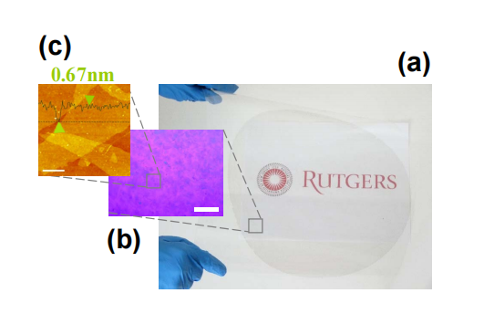
The deposition of atomically thin highly uniform chemically derived graphene (CDG) films on 300 mm SiO2/Si wafers is reported. We demonstrate that the very thin films can be lifted off to form uniform membranes than can be free-standing or transferred onto any substrate. Detailed maps of thickness using Raman spectroscopy and atomic force microscopy (AFM) height profiles reveal that the film thickness is very uniform and highly controllable, ranging from 1-2 layers up to 30 layers. After reduction using a variety of methods, the CDG films are transparent and electrically active with FET devices yielding exceptionally high mobilities of ~ 15 cm2 /Vs and sheet resistance of ~ 1 kΩ/sq at ~ 70 % transparency.
Graphene is emerging as a promising material that has the potential to revolutionize materials physics as well as much of present day electronics. While graphene could be viewed as the material for next generation of electronics, reports on making it technologically feasible for integration into devices are only recently beginning to emerge. It is important to recognize that the extra-ordinary fundamental properties of a novel material do not necessarily translate into technological innovations and eventual implementation into applications. For example, it is useful to note that despite the investment of large amount of effort and resources over nearly two decades along with their attractive properties, single walled carbon nanotubes (SWNTs) have not been implemented into mainstream nano-electronics due to the absence of large area deposition and device integration due to lack of control over chirality and organization. Instead, large area or macro-electronics applications on flexible substrates requiring moderate performance devices where solution processed networks of SWNTs can be utilized have recently gained prominence.6-7 Graphene will face similar challenges and thus it is important to tackle the obstacles of large area deposition and integration at an early stage of its development. In contrast to one dimensional nanomaterials, the synthesis of high quality graphene films on large area, CMOS compatible substrates will allow device fabrication using the well-known micro-electronics paradigm for thin film processing driven by continuing progress in lithography (top down approach). This represents a clear advantage over other materials that require novel approaches for their organization in dense arrays, capable of yielding device densities competitive with ULSI requirements.
There are two approaches to ultra-large area deposition of graphene. The first approach deals with condensation of high quality graphene with controllable layers using chemical vapor deposition (CVD) for nano-electronics where materials with extra-ordinary mobility values are required. The CVD approach requires high temperatures and single crystal substrates, although recent progress on growth and transfer suggests that graphene on a variety of substrates is feasible.5,8-10 The second approach, the topic of this contribution, is the utilization of large area deposition of chemically derived graphene (CDG) from solution for electronics where extraordinary electrical properties are not required for high performance devices on flexible platforms. Devices such as sensors, nanoelectromechnical systems (NEMS), transparent conductors, transistors, and field emitters, along with potential photonic applications have been demonstrated with CDG. Virtually all such devices require peripheral CMOS based components for logic and operation. For example, existing tin oxide based sensors utilize lithographically processed heaters which enhance the sensitivity as well as refresh the sensing material. Thus, 300 mm (a size compatible with existing CMOS tools) wafer scale deposition of highly uniform CDG thin films with controllable number of layers is the first step towards technological implementation.

Fig1
A schematic of the lift-off and transfer procedure of the thin films to obtain free-standing membranes is also shown in Figure 1 (a). The successful transfer of one dimensional nanostructures has been demonstrated over reasonably large areas.26-28 The advantage of the method reported here is that it can transfer very uniform CDG thin films on 300 mm wafers with yield of 100 %. This procedure leads to uniform lift-off of membranes consisting of atomically thin CDG films with poly meta methyl acrylate (PMMA) support, which can be readily handled as bulk film. Pure CDG membranes can be transferred onto any substrate by scooping or remain free-standing after PMMA removal using solvents such as acetone. Furthermore, we did not observe cracks on our transferred films, which are reported to be present in the transferred CVD-grown graphene films. The ability to fabricate free-standing CDG films indicates that the individual flakes within the thin films are well adhered and form a continuous network, which allows the membranes to maintain structural integrity even when the support PMMA is washed away. Photographs of 150 mm and 300 mm wafers (6 and 12 inches) with atomically thin layers of uniform CDG and the corresponding free-standing membranes are shown in Figure 1 (b) and (c), respectively.
Raman spectroscopy was performed to confirm the thickness of the thin films by measuring the number of reduced CDG layers. Raman spectra of reduced CDG membrane were similar to our previous results4 in that it showed the presence of the usual D, G, and 2D peaks. Presence of D peak, which is absent in mechanically cleaved graphene, indicates the presence of structural imperfections induced by the attachment of oxygen functional groups on the carbon basal plane. The intensity of the 2D peak with respect to the D and G peaks is small due to disorder but the shift and shape of this peak can be used for analyzing the number of layers in reduced CDG. We have performed similar analysis to our previous work4 to determine the number layers in reduced CDG thin films. A typical Raman map over 48 μm x 24 μm spatial region is shown in Figure 2 (d). The result shows that the thin films deposited consist of mostly single to bi-layer, which is consistent with AFM image in Figure 2 (c).
下一篇: 表面声波器件在碳化硅上使用铌酸锂