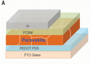
State-of-the-art photovoltaics use high-purity, large-area, wafer-scale single-crystalline semiconductors grown by sophisticated, high-temperature crystal growth processes. We demonstrate a solution-based hot-casting technique to grow continuous, pinhole-free thin films of organometallic perovskites with millimeter-scale crystalline grains. We fabricated planar solar cells with efficiencies approaching 18%, with little cell-to-cell variability. The devices show hysteresis-free photovoltaic response, which had been a fundamental bottleneck for the stable operation of perovskite devices. Characterization and modeling attribute the improved performance to reduced bulk defects and improved charge carrier mobility in large-grain devices. We anticipate that this technique will lead the field toward synthesis of wafer-scale crystalline perovskites, necessary for the fabrication of high-efficiency solar cells, and will be applicable to several other material systems plagued by polydispersity, defects, and grain boundary recombination in solution-processed thin films.
Our method leads to grain sizes as large as 1 to 2 mm, in comparison with the grain sizes of ~1 to 2 mm typically obtained using the conventional post-annealing process. (See fig. S4 for details of the average grain size calculation procedure.) The major difference between hot-casting and conventional post-annealing is the presence of solvent when heating the substrate. For hot-casting, there is excess solvent present when the substrate is maintained above the crystallization temperature for the formation of the perovskite phase. This allows for the prolonged growth of the perovskite crystals, yielding large crystalline grains. Thus, the use of high–boiling point solvents (see Fig. 1C) provides the ideal conditions for the growth of large crystalline grains, as the excess solvent allows more time for their growth (24) (fig. S5).
Optical images (Fig. 1, B and C) and SEM images (fig. S2) illustrate that the perovskite thin films produced with the hot-casting method (from 100°C up to 180°C) are uniform, pinhole-free, and cover the entire substrate. We also used highresolution SEM imaging to evaluate the morphology of the large- and small-area grains and found that except for the size of the grain, there was no observable difference in micromorphology (fig. S2). Preliminary analysis using high-resolution crosssectional SEM imaging coupled with optical polarization microscopy and photoluminescence spectral imaging (figs. S18 to S20) shows consistency of the bulk single-crystalline nature over a large area of the perovskite film. The hot-casting method is applicable for both pure and mixedhalide perovskite combinations (fig. S6) and may lead to the realization of industrially scalable large-area crystalline thin films made from other materials [such as copper zinc tin sulfide (CZTS), copper indium gallium selenide (CIGS), and cadmium telluride (CdTe)] by means of low-temperature, solution-processed, large-area crystal growth.

Fig1
Optical images (Fig. 1, B and C) and SEM images (fig. S2) illustrate that the perovskite thin films produced with the hot-casting method (from 100°C up to 180°C) are uniform, pinhole-free, and cover the entire substrate. We also used highresolution SEM imaging to evaluate the morphology of the large- and small-area grains and found that except for the size of the grain, there was no observable difference in micromorphology (fig. S2). Preliminary analysis using high-resolution crosssectional SEM imaging coupled with optical polarization microscopy and photoluminescence spectral imaging (figs. S18 to S20) shows consistency of the bulk single-crystalline nature over a large area of the perovskite film. The hot-casting method is applicable for both pure and mixedhalide perovskite combinations (fig. S6) and may lead to the realization of industrially scalable large-area crystalline thin films made from other materials [such as copper zinc tin sulfide (CZTS), copper indium gallium selenide (CIGS), and cadmium telluride (CdTe)] by means of low-temperature, solution-processed, large-area crystal growth.
High-performance cells have previously been reported with micrometer-sized grains (1, 26–28). We believe that there are two primary benefits of growing crystals with large grain size: (i) The reduced interfacial area associated with large grains suppresses charge trapping and eliminates hysteresis (irrespective of the direction of voltage sweep or the scan rate), and (ii) larger grains have lower bulk defects and higher mobility, allowing for the photogenerated carriers to propagate through the device without frequent encounters with defects and impurities.